The world of electronics is filled with acronyms and seemingly cryptic terms. Today, we’re diving into one of the foundational building blocks: the DIP, or Dual In-line Package.
For decades, DIPs reigned supreme as the go-to package for housing integrated circuits (ICs), the tiny chips that power our devices. But what exactly is a DIP, and how does it work? In this blog post, we’ll unveil the mysteries of the DIP, exploring its design, function, and its place in the history of electronics.
What Is Dip Integrated Circuit?
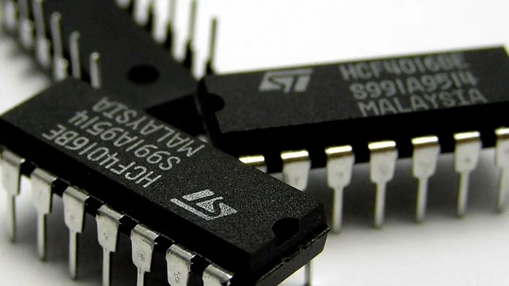
A DIP (Dual In-Line Package) integrated circuit (IC) is essentially a chip wrapped up for business in the electronics world. Let’s break it down:
- Dual In-Line: This refers to the physical shape. Imagine a rectangular package with two rows of electrical connectors (pins) running along the sides, like legs.
- Package: This is the housing that protects the delicate integrated circuit (IC) inside. ICs are tiny marvels of engineering, but they’re also fragile. The package shields the chip from damage and provides a way to connect it to other components in a circuit.
So, a DIP IC is a self-contained unit housing an IC chip, ready to be plugged into a circuit board.
History of DIP Package
The DIP package boasts a rich history, playing a pivotal role in the evolution of electronics. Here’s a glimpse into its past:
- Origins (1960s): Prior to the DIP, integrated circuits (ICs) were often housed in bulky metal cans with limited connection points. In the mid-1960s, engineers at Fairchild Semiconductor, namely Don Forbes, Rex Rice, and Bryant Rogers, saw a need for a more practical solution. They developed the first 14-lead ceramic DIP in 1964.
- Revolutionizing Design (1970s): The DIP’s rectangular shape with two rows of pins offered several advantages. It simplified circuit board layout, allowed for automated assembly, and provided a more compact design compared to previous packages. This innovation significantly reduced production costs and paved the way for mass production of electronic devices.
- Material Shift (1970s): Initially, DIPs were made from ceramic for their durability. However, by the late 1970s, plastic DIPs (PDIPs) emerged as a more cost-effective option for less demanding applications. PDIPs quickly became the dominant type due to their lower cost and lighter weight.
- Rise of SMT (1980s onwards): As technology progressed, the need for even smaller and higher-density circuits grew. In the 1980s, Surface-Mount Technology (SMT) packages started gaining traction. SMT components, like SOICs (Small-Outline Integrated Circuits), could be soldered directly onto the surface of the circuit board, offering significant space savings.
- DIP’s Legacy: While DIPs have largely been replaced by SMT packages in high-volume consumer electronics, they remain a valuable tool for hobbyists, prototyping, and specific industrial applications. Their ease of use, familiarity, and availability across a wide range of ICs make them a continuing favorite for many electronic tinkerers and learners.
Types of Dual Inline Packages
There are a few variations of the classic DIP package, each catering to specific needs:
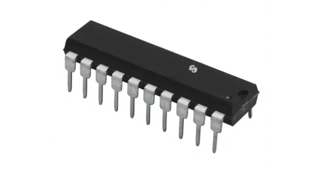
Plastic Dual In-Line Package (PDIP): This is the most common and recognizable DIP type. It features a black plastic body and is the workhorse for many hobbyist circuits.
Ceramic Dual In-Line Package (CERDIP or CDIP): When higher durability or heat resistance is required, ceramic is used for the package. CERDIPs are slightly larger than PDIPs and are often used in industrial or military applications due to their sturdiness.
Shrink Plastic Dual In-Line Package (SPDIP): As miniaturization became a priority, the SPDIP emerged. It maintains the DIP design but with a narrower body and tighter pin spacing to save on space on circuit boards.
Skinny Dual In-Line Package (SDIP): Similar to the SPDIP, the SDIP offers a slimmer profile but with a standard DIP pin spacing. This provides a space-saving option while maintaining compatibility with existing DIP layouts.
Dual Inline Package Structure
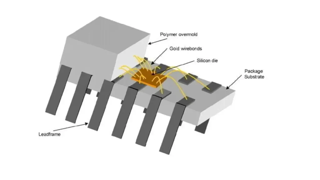
A Dual In-line Package (DIP) is a type of housing for electronic components, particularly integrated circuits (ICs). Here’s a breakdown of its structure:
Shape and Material:
- Rectangular plastic casing made of epoxy resin (most common) or ceramic (for high temperatures or special needs).
- Inside, a lead frame made of metal (tin, silver, or gold plated) holds the actual electronic chip and provides connection points.
Pins:
- Two rows of metal pins run parallel to each other on either long side of the rectangle.
- The number of pins varies depending on the component and its complexity (common counts include 8, 14, 16, 40).
- Pin spacing and row spacing are standardized for easy integration into circuits (typically 0.1 inch pin pitch and 0.3 or 0.6 inch row spacing).
- There’s usually a notch or indentation on one end of the package to indicate pin 1 for proper orientation.
Mounting:
- DIPs are traditionally mounted on a Printed Circuit Board (PCB) using through-hole technology.
- The pins are inserted into holes drilled on the PCB and then soldered to create electrical connections.
- Alternatively, DIPs can be plugged into sockets soldered onto the PCB, allowing for easier removal or replacement of the component.
Applications:
- While less common in modern electronics due to smaller surface-mount technology, DIPs are still used in various applications:
- Older electronic devices
- Prototyping circuits
- Hobbyist electronics
- Components needing occasional replacement (e.g., DIP switches)
I hope this explanation clarifies the structure of a Dual Inline Package!
Pros and Cons of Dual Inline Package
Pros of DIPs:
- Cost-effective: Simple design and mature manufacturing process make DIPs generally less expensive than some newer packaging options.
- Easy Assembly: Through-hole mounting with larger pins simplifies manual assembly, making them ideal for prototyping and small-batch production.
- Durable: Larger size and rigid construction offer good mechanical strength and can withstand some vibration or stress.
- Easy Replacement: Components can be easily removed and replaced, especially when using sockets, which is beneficial for troubleshooting or repairs.
- Good Heat Dissipation: Larger package size allows for better heat dissipation compared to some miniaturized packages.
- Wide Availability: DIPs are still widely available for a large variety of components.
Cons of DIPs:
- Large Footprint: DIPs take up more space on a PCB due to their size and pin spacing, limiting their use in high-density applications.
- Lower Performance: Parasitic capacitance and inductance from the leads can limit their performance at high frequencies.
- Limited Automation: Traditional through-hole mounting requires specialized equipment that not all factories have, making automated assembly more challenging.
- Obsolescence: As technology advances, some DIP components may become harder to source in the future.
- Weaker Strength: DIPs can be susceptible to damage from bending or twisting compared to some newer, sturdier packages.
DIPs offer advantages in cost, ease of use, and durability, making them well-suited for prototyping, hobbyist electronics, and applications where space is not a major constraint. However, their larger size and lower performance make them less ideal for modern, high-density electronic devices.
Pins of DIP
The pins of a Dual In-line Package (DIP) are the metal legs that protrude from the long sides of the rectangular package. They provide electrical connections between the integrated circuit (IC) inside the DIP and the circuit board it’s mounted on.
Number of Pins:
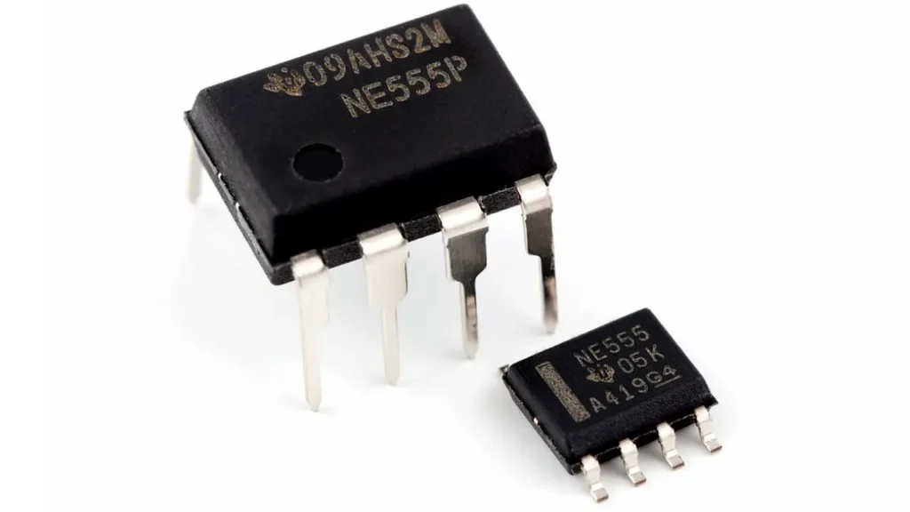
The number of pins on a DIP varies depending on the complexity of the IC it houses. Common DIP pin counts include:
- 8
- 14
- 16
- 40
Pin Arrangement:
The pins are arranged in two parallel rows on either long side of the rectangle. The spacing between the pins (pitch) and the spacing between the rows are standardized for easy integration into circuits. Typically, there’s a 0.1 inch pin pitch and 0.3 or 0.6 inch row spacing.
Pin 1 Indicator:
One end of the DIP package usually has a notch or indentation to indicate pin 1. This is crucial for ensuring proper orientation of the component when inserting it into the circuit board. Proper orientation is necessary because the pins have specific functions assigned to them, and following the pinout diagram (which designates the function of each pin) is essential for the circuit to function correctly.
Soldering the Pins:
DIPs are traditionally mounted on a Printed Circuit Board (PCB) using through-hole technology. The pins are inserted into holes drilled on the PCB and then soldered to create electrical connections. Alternatively, DIPs can be plugged into sockets soldered onto the PCB, allowing for easier removal or replacement of the component.
Electrical Characteristics of DIP Components
DIP components themselves don’t have inherent electrical characteristics like resistance, capacitance, or voltage ratings. Those characteristics depend on the specific electronic component housed within the DIP package. However, the pins of a DIP can introduce some electrical effects to consider:
- Parasitic Capacitance and Inductance: The DIP’s leads act as small capacitors and inductors. This can become significant at high frequencies, potentially affecting signal integrity and causing issues like ringing or crosstalk. Surface-mount technology (SMT) components generally have shorter leads and less parasitic capacitance/inductance, making them preferable for high-frequency applications.
- Voltage and Current Ratings: While the DIP package itself doesn’t have voltage or current ratings, the individual component inside (IC, resistor, etc.) will have its own specifications. It’s crucial to consult the datasheet for the specific component to ensure you’re operating it within its voltage and current limits.
Additional Considerations:
- Power Dissipation: DIP packages, particularly those made of plastic, might have limitations on how much heat they can dissipate compared to some metal packages used in SMT components. This can be a factor when choosing components for high-power applications.
- Grounding: Proper grounding practices are important for any circuit, and DIP components are no exception. Some DIP ICs might have dedicated ground pins for optimal performance.
DIP vs SOIC
Dual In-Line Package (DIP) and Small Outline Integrated Circuit (SOIC) are two common types of packages used to house integrated circuits (ICs). Here’s a breakdown of their key differences:
| Feature | DIP | SOIC |
|---|---|---|
| Shape | Rectangular with two rows of pins on long sides | Rectangular with gull-wing shaped leads on bottom |
| Size | Larger footprint | Smaller footprint |
| Mounting | Through-hole technology (pins inserted into PCB holes) | Surface-mount technology (soldered directly to PCB surface) |
| Assembly | Easier for manual assembly | Requires precise soldering techniques or pick-and-place machines |
| Durability | More resistant to physical damage | More delicate, susceptible to bending or breaking leads |
| Cost | Generally less expensive | Can be slightly more expensive |
| Performance | May have limitations at high frequencies due to pin inductance/capacitance | Generally better high-frequency performance |
| Availability | Widely available for many components | May be less available for newer components |
| Applications | Prototyping, hobbyist electronics, older devices, applications requiring easy component replacement | High-density PCBs, modern electronics, mass-produced devices |
DIPs are a mature and user-friendly option, ideal for prototyping, hobbyists, and applications where space is not a major concern. SOICs offer a more compact, higher-performance solution for modern, miniaturized electronics.
Additional Considerations:
- Number of Pins: Both DIP and SOIC come in various pin counts to accommodate different ICs.
- Heat Dissipation: DIPs generally have better heat dissipation due to their larger size.
- Environmental Concerns: Lead-free options are available for both DIP and SOIC to comply with environmental regulations.
Choosing between DIP and SOIC depends on your specific needs and priorities. Consider factors like project requirements, component availability, and your skillset for assembly.
Conclusion
Dual In-Line Packages (DIPs) have been a mainstay in electronics for decades, valued for their simplicity, affordability, and ease of use. Their larger size makes them ideal for prototyping, hobbyist projects, and applications where components need occasional replacement. However, as technology advances, DIPs are gradually being replaced by smaller, surface-mount technology (SMT) components in high-density modern devices.
Here’s a quick recap of DIPs:
- Cost-effective and Easy to Use: Simple design and traditional through-hole mounting make DIPs economical and well-suited for manual assembly.
- Durable: Their larger size and rigid construction offer good mechanical strength.
- Easy Replacement: Components can be easily removed and replaced, especially with sockets.
However, DIPs also have some limitations:
- Larger Footprint: DIPs take up more space on a PCB, limiting their use in compact devices.
- Lower Performance: Leads can introduce parasitic capacitance and inductance, hindering performance at high frequencies.
- Obsolescence: Some DIP components may become harder to source in the future.
So, when should you use DIPs?
- Prototyping and hobbyist electronics
- Circuits where space isn’t a major concern
- Applications requiring occasional component replacement
Ready to incorporate DIPs into your next project? Weishi Electronics offers a wide range of DIP integrated circuits at competitive prices. Contact us now today to get a quote and find the perfect DIP components for your needs!