A diode, a fundamental component in electronics, serves as a one-way gate for electric current. This tiny yet essential device is crafted from materials that exhibit specific electrical properties, enabling it to control the flow of current with remarkable precision.
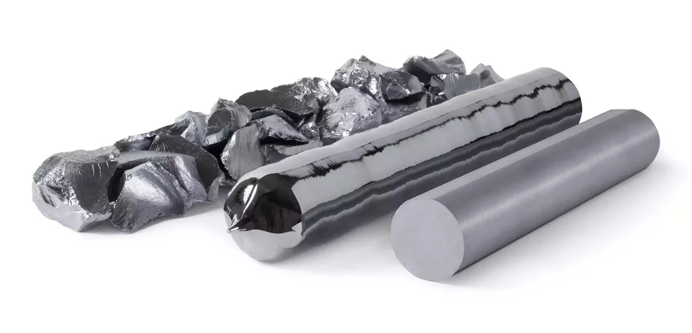
Diodes are primarily made of semiconductor materials, most commonly silicon and germanium. Understanding their composition and structure reveals their critical role in various electronic circuits.
What Is A Diode?
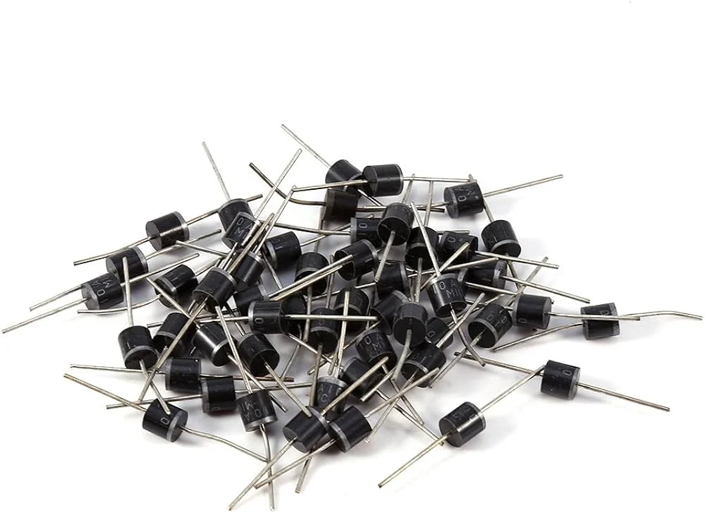
A diode, a specialized electronic device, possesses two terminals known as the anode and cathode. Typically crafted from semiconductor materials like silicon, germanium, or selenium, although certain diodes feature metal electrodes enclosed within a chamber either emptied or filled with a low-pressure pure elemental gas. Diodes serve various functions such as rectification, signal limitation, voltage regulation, switching, modulation, mixing, demodulation, and oscillation in electronic circuits.
What Is A Diode Made Of?
A diode is a semiconductor device that allows current to flow in one direction while blocking it in the opposite direction. This functionality is achieved through the careful composition and structure of the diode, which involves the use of specific semiconductor materials and the formation of a p-n junction. Let’s expand on these components in detail.
Semiconductor Materials
1. Silicon
Silicon is the most widely used semiconductor material for diodes. It has excellent electrical properties, including a suitable band gap of about 1.1 eV at room temperature. This band gap allows silicon to effectively control the flow of current, making it ideal for a wide range of electronic applications.
Silicon diodes are known for their robustness, high-temperature tolerance, and durability. These characteristics make silicon diodes suitable for high-power and high-frequency applications. Additionally, silicon is abundant and relatively inexpensive, contributing to its widespread use in the electronics industry.
2. Germanium
Germanium is another semiconductor material used in diodes, though it is less common than silicon. Germanium has a smaller band gap of about 0.66 eV, which makes it more sensitive to temperature changes and less suitable for high-temperature environments.
Germanium diodes are characterized by a lower forward voltage drop (approximately 0.3 volts) compared to silicon diodes (approximately 0.7 volts). This property makes germanium diodes useful in applications where a low forward voltage drop is essential, such as in certain radio frequency and signal detection circuits.
Despite its advantageous electrical properties, the higher cost and lower thermal stability of germanium limit its use compared to silicon.
Junction Formation
The functional aspect of a diode comes from the formation of a p-n junction, which is created by doping the semiconductor material to produce distinct regions with different electrical properties.
Donor And Acceptor Regions
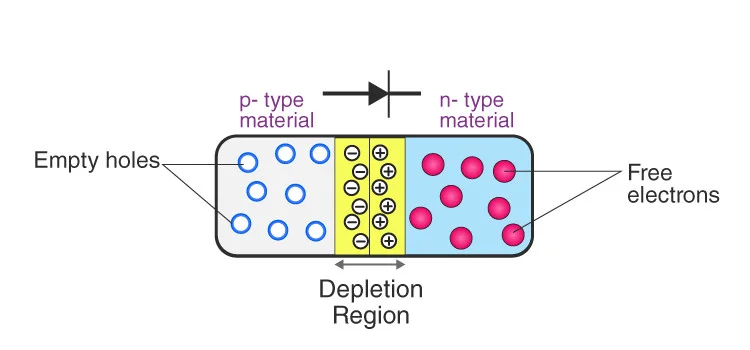
The p-n junction is formed by combining two types of semiconductor regions: the p-type and the n-type. The p-type region is created by doping the semiconductor with acceptor impurities, which introduce holes (positive charge carriers) into the material. Common acceptor impurities include elements from group III of the periodic table, such as boron.
The n-type region is formed by doping the semiconductor with donor impurities, which provide extra electrons (negative charge carriers). Common donor impurities include elements from group V of the periodic table, such as phosphorus.
This interface where these two regions meet is known as the p-n junction. At this junction, electrons from the n-type region diffuse into the p-type region and recombine with holes, creating a depletion region that acts as a barrier to charge carrier movement.
Creation Of One-Way Pathway For Current Flow
The p-n junction establishes a unidirectional pathway for current, which is the defining characteristic of a diode. Applying a forward voltage (positive to the p-type and negative to the n-type) narrows the depletion region, permitting current to pass through the diode. Conversely, applying a reverse voltage (negative to the p-type and positive to the n-type) widens the depletion region, halting current flow. This characteristic allows current to flow in one direction while blocking it in the opposite direction.
The diode’s rectifying property finds applications in various fields, including converting alternating current (AC) to direct current (DC), signal demodulation, and safeguarding circuits from reverse polarity.
To sum up, a diode’s construction involves using semiconductor materials like silicon and germanium and forming a p-n junction through doping to create donor and acceptor regions. This arrangement empowers the diode to regulate the direction of current flow, rendering it a vital element in numerous electronic devices.
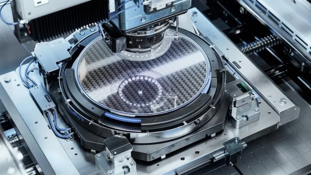
How Is A Diode Made?
Wafer Preparation
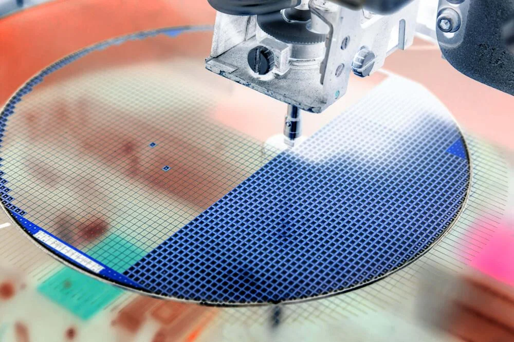
The journey of creating a diode starts with the careful selection of a high-purity semiconductor wafer, typically crafted from silicon owing to its exceptional electrical properties. This pristine wafer undergoes a meticulous preparation process, where it is subjected to thorough cleaning and precision polishing to eliminate any impurities and rectify surface defects.
Each step in this process is executed with utmost precision and attention to detail, ensuring that the wafer emerges as a flawless canvas, ready to undergo further fabrication steps. This initial preparation lays the foundation for the creation of high-quality diodes with reliable performance and durability.
Doping
The subsequent stage includes doping the semiconductor wafer to generate the essential p-type and n-type regions for forming the p-n junction. To create the p-type region, acceptor impurities like boron are doped into the wafer. This action introduces “holes” into the silicon lattice, generating a positively charged area.
For the n-type region, the wafer is doped with donor impurities, such as phosphorus. This introduces excess electrons into the silicon lattice, creating a negatively charged region. The doping process is typically accomplished through techniques such as ion implantation or diffusion, where the dopant atoms are introduced into the semiconductor material and then diffused to the desired depth.
Photolithography
Photolithography is used to define the specific patterns and structures on the semiconductor wafer. This process involves applying a photoresist material to the wafer’s surface and then exposing it to ultraviolet light through a mask.
The mask contains the desired patterns for the diode’s features, such as the metal contacts and the isolation areas between devices. The exposed photoresist material undergoes a chemical reaction, allowing it to be selectively removed.
Etching
After photolithography, the semiconductor wafer undergoes etching to remove the exposed areas of the semiconductor material not protected by the photoresist. Chemical etchants are used to selectively dissolve the semiconductor material, leaving behind the patterned regions defined by the photoresist.
Metal Deposition
Metal deposition is carried out to create the metal contacts necessary for connecting the diode to external circuitry. Thin layers of metal (such as aluminum or gold) are deposited onto the semiconductor wafer’s surface using techniques like sputtering or evaporation. These metal layers form electrical contacts with the doped semiconductor regions, providing terminals for connecting the diode to external electrical components.
Passivation And Encapsulation
In order to safeguard the diode from environmental influences and guarantee its enduring dependability, layers of passivation and encapsulation are administered. Passivation entails the application of a thin insulating layer (such as silicon dioxide or silicon nitride) onto the diode’s surface, shielding it from moisture and impurities. Encapsulation involves enclosing the diode in a protective casing, usually crafted from plastic or ceramic, to furnish both mechanical reinforcement and electrical insulation.
Testing And Sorting
Finally, the fabricated diodes undergo rigorous testing to ensure they meet the required electrical specifications and performance criteria. Diodes that pass the testing process are sorted and packaged for distribution to customers, while defective ones are discarded.
How To Make A Homemade Diode?
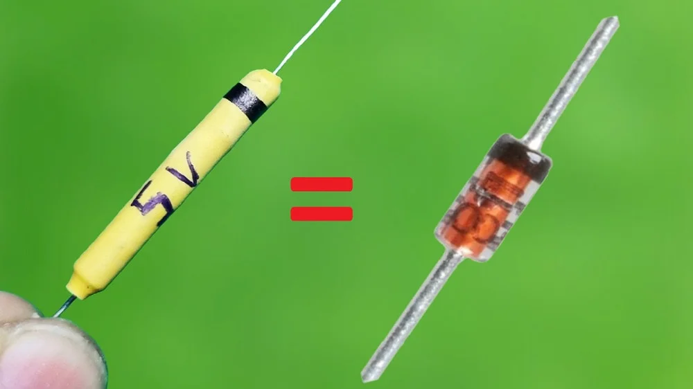
Making a homemade diode can be a fun and educational project, though it may not yield a highly efficient or reliable component compared to commercially manufactured diodes. Here’s a basic method to create a simple diode using readily available materials:
Materials Needed: Copper Wire, Pencil with Graphite Core, Small Piece of Cardboard or Plastic
Battery, Alligator Clips, or Wires.
1. Prepare The Copper Wire
Take a copper wire measuring approximately 5 to 10 centimeters in length. Employ a wire stripper or a small knife to remove around 1 centimeter of insulation from both ends, ensuring not harm to the copper strands. After stripping, examine the exposed copper to confirm its cleanliness and absence of debris.
If required, twist the copper strands together securely. Your copper wire is now prepared for utilization in crafting the homemade diode.
2. Create The Anode And Cathode
Preparing the copper wire for constructing the homemade diode, take one end of the wire and carefully bend it into a small loop or hook. This looped end will serve as the anode, or positive terminal, of the diode. Use a pair of needle-nose pliers to make the loop, ensuring it is tight and secure, yet large enough to facilitate a good electrical connection. Meanwhile, leave the opposite end of the wire straight.
This straight end will act as the cathode, or negative terminal, of the diode. Ensure both ends are free of any insulation and any sharp edges or burrs that could interfere with their functionality. By creating a loop at one end and leaving the other end straight, you clearly define the anode and cathode terminals, which are crucial for the proper directional flow of current in your homemade diode.
3. Prepare The Graphite Core
To prepare the copper wire for constructing the homemade diode, take one end of the wire and carefully bend it into a small loop or hook. This looped end will serve as the anode, or positive terminal, of the diode. Use a pair of needle-nose pliers to make the loop, ensuring it is tight and secure, yet large enough to facilitate a good electrical connection.
Meanwhile, leave the opposite end of the wire straight. This straight end will act as the cathode, or negative terminal, of the diode. Ensure both ends are free of any insulation and any sharp edges or burrs that could interfere with their functionality. By creating a loop at one end and leaving the other end straight, you clearly define the anode and cathode terminals.
4. Attach The Components
Assemble the homemade diode, and secure the copper wire (anode) and the graphite core (cathode) onto a small piece of cardboard or plastic. Position the copper wire on one side with the looped end facing outward, and place the graphite core on the opposite side, leaving a small gap between them to prevent direct contact.
Use tape or glue to attach them firmly to the base, ensuring the tape or glue does not cover the gap. This setup establishes a stable foundation with clearly defined anode and cathode, essential for the diode’s proper functioning and integrity during testing and use.
5. Testing
To test the homemade diode, connect one end of the copper wire (the anode) to the positive terminal of the battery and connect the graphite core (the cathode) to the negative terminal of the battery. Use alligator clips or wires to securely make these connections.
If the diode is constructed correctly, it will permit current to flow from the anode to the cathode, demonstrating forward bias, but will block current flow in the opposite direction, indicating reverse bias.
Important Notes:
The homemade diode may not exhibit the same performance characteristics as commercial diodes, potentially having a higher forward voltage drop and lower efficiency. Its effectiveness can vary depending on the materials used and the construction technique.
When working with batteries and electrical components, exercise caution to avoid injury or damage. This project is primarily educational and may not be suitable for practical applications requiring reliable diodes.
Conclusion
In essence, the makeup of a diode plays a crucial role in its operation within electronic circuits. By carefully choosing semiconductor materials such as silicon or germanium and creating specific p-n junctions, diodes precisely control current flow.
Grasping the composition of diodes provides an understanding of the synergy between material science and electrical engineering, which fuels advancements in semiconductor technology.