Semiconductors have become the backbone of modern electronics, enabling the remarkable technological advancements that have transformed our lives. From the smartphones in our pockets to the advanced medical equipment in hospitals, these remarkable materials are the foundation upon which the digital revolution has been built.
However, the world of semiconductors is far more diverse than the ubiquitous silicon chip. In fact, there are several distinct types of semiconductor materials, each with its own unique properties and applications. Understanding these different semiconductor types is crucial for appreciating the breadth and depth of their impact on technology.
In this blog post, we will delve into the fascinating world of semiconductors, exploring the various categories that have shaped the landscape of electronics. From the well-established intrinsic and extrinsic semiconductors to the emerging realm of compound and organic semiconductors, we will uncover the distinctive characteristics and use cases of each type.
What Are Semiconductors
Semiconductors are materials that have electrical conductivity properties that fall between those of conductors (such as metals) and insulators (such as glass or plastic). They are the fundamental building blocks of modern electronics and have revolutionized the way we interact with technology.
How Many Types of Semiconductors Are There
There are several main types of semiconductors, which can be broadly categorized as follows:
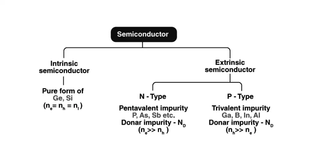
Intrinsic Semiconductors:
- These are pure semiconductor materials, such as silicon (Si) and germanium (Ge), that have a crystal-like atomic structure with four valence electrons.
Extrinsic Semiconductors:
Doped Semiconductors:
These are intrinsic semiconductors that have been doped with small amounts of impurities, creating either n-type (excess electrons) or p-type (excess holes) semiconductors.
PN Junctions:
When n-type and p-type semiconductors are joined together, they form a PN junction, which is the fundamental building block of many electronic devices like diodes and transistors.
Compound Semiconductors:
III-V Compound Semiconductors:
- These are formed by combining elements from group III (e.g., gallium, indium) and group V (e.g., arsenic, phosphorus) of the periodic table, such as gallium arsenide (GaAs) and indium phosphide (InP).
- II-VI Compound Semiconductors:
- These are formed by combining elements from group II (e.g., zinc, cadmium) and group VI (e.g., oxygen, sulfur, selenium, tellurium) of the periodic table, such as cadmium telluride (CdTe) and zinc oxide (ZnO).
Organic Semiconductors:
- These are made from carbon-based organic compounds, such as conjugated polymers and small organic molecules, that exhibit semiconductor properties.
In addition to these major categories, there are also some other specialized types of semiconductors, such as:
- Wide-bandgap Semiconductors (e.g., gallium nitride, silicon carbide)
- Amorphous Semiconductors (e.g., amorphous silicon)
- Quantum Dot Semiconductors
The diversity of semiconductor types, each with its own unique properties and applications, has been instrumental in the development of a wide range of electronic devices and technologies, from integrated circuits and optoelectronics to power electronics and flexible electronics.
Types of Semiconductor
Here are the main types of semiconductors:
1. Intrinsic Semiconductors:
Intrinsic semiconductors are pure semiconductor materials that have not been doped with any impurities. They exhibit semiconductor properties due to the inherent characteristics of their atomic structure.
Silicon (Si) as an Intrinsic Semiconductor
Silicon is the most widely used intrinsic semiconductor material. It has a diamond-like crystal structure, where each silicon atom is covalently bonded to four neighboring silicon atoms.
Key Properties of Silicon as an Intrinsic Semiconductor:
- Atomic Structure: Silicon has four valence electrons, which allows it to form strong covalent bonds with its neighboring atoms, creating a stable crystal structure.
- Electrical Conductivity: At room temperature, silicon has a moderate number of charge carriers (electrons and holes) that can move through the material and conduct electricity. However, this number is relatively low compared to metals.
- Bandgap Energy: Silicon has an energy bandgap of approximately 1.12 eV, which is the energy required to excite an electron from the valence band to the conduction band. This bandgap energy is responsible for silicon’s semiconductor behavior.
- Intrinsic Carrier Concentration: The intrinsic carrier concentration (ni) in silicon is around 1.5 × 10^10 cm^-3 at room temperature. This refers to the number of electron-hole pairs present in the material without any external doping.
- Mobility: Silicon has relatively high electron and hole mobilities, which are measures of how quickly charge carriers can move through the material under an applied electric field.
Germanium (Ge) as an Intrinsic Semiconductor
Germanium is another important intrinsic semiconductor material. Like silicon, germanium has a diamond-like crystal structure and can conduct electricity due to the presence of charge carriers.
Key Properties of Germanium as an Intrinsic Semiconductor:
- Atomic Structure: Germanium, similar to silicon, has a diamond-like crystal structure with each germanium atom covalently bonded to four neighboring germanium atoms.
- Electrical Conductivity: Germanium has higher electrical conductivity compared to silicon, with a lower energy bandgap of approximately 0.67 eV.
- Intrinsic Carrier Concentration: The intrinsic carrier concentration in germanium is much higher than in silicon, around 2.4 × 10^13 cm^-3 at room temperature.
- Mobility: Germanium has higher electron and hole mobilities compared to silicon, making it more suitable for high-speed electronic applications.
The unique properties of intrinsic semiconductors, such as silicon and germanium, have been instrumental in the development of various electronic devices and technologies. However, the limited number of charge carriers in intrinsic semiconductors has led to the development of extrinsic semiconductors, which are created by intentionally doping the material with impurities to enhance its electrical properties.
2. Extrinsic Semiconductors:
Extrinsic semiconductors are semiconductor materials that have been intentionally doped with small amounts of impurities to enhance their electrical properties. This process of doping introduces additional charge carriers (electrons or holes) into the semiconductor, which significantly alters its behavior compared to intrinsic semiconductors.
There are two main types of extrinsic semiconductors:
- N-type Semiconductors
- P-type Semiconductors
N-type Semiconductors
N-type semiconductors are created by doping an intrinsic semiconductor, such as silicon or germanium, with a group V element, like phosphorus (P), arsenic (As), or antimony (Sb).
Key Characteristics of N-type Semiconductors:
- Impurity Atoms: The group V impurity atoms have five valence electrons, one more than the four required for covalent bonding in the semiconductor’s crystal structure.
- Excess Electrons: The extra electron from the impurity atom is not needed for covalent bonding and becomes a free electron, contributing to the semiconductor’s conduction.
- Majority Charge Carriers: In an n-type semiconductor, the majority charge carriers are the excess free electrons, making them the dominant charge carriers responsible for electrical conduction.
- Increased Conductivity: The presence of these excess free electrons significantly increases the electrical conductivity of the n-type semiconductor compared to an intrinsic semiconductor.
P-type Semiconductors
P-type semiconductors are created by doping an intrinsic semiconductor with a group III element, such as boron (B), aluminum (Al), or gallium (Ga).
Key Characteristics of P-type Semiconductors:
- Impurity Atoms: The group III impurity atoms have three valence electrons, one less than the four required for covalent bonding in the semiconductor’s crystal structure.
- Hole Formation: The missing electron in the covalent bond creates a “hole,” which can be thought of as a positive charge carrier.
- Majority Charge Carriers: In a p-type semiconductor, the majority charge carriers are the holes, making them the dominant charge carriers responsible for electrical conduction.
- Increased Conductivity: The presence of these holes significantly increases the electrical conductivity of the p-type semiconductor compared to an intrinsic semiconductor.
The combination of n-type and p-type semiconductors forms the fundamental building block of many electronic devices, known as the PN junction. This junction is the basis for diodes, transistors, and integrated circuits, which are the core components of modern electronics.
By carefully controlling the doping process, engineers can precisely tailor the electrical properties of semiconductors to meet the specific requirements of various electronic applications, from digital logic circuits to power electronics and optoelectronic devices.
3. Compound Semiconductors:
Compound semiconductors are materials that are formed by combining two or more elements, often from the III-V or II-VI groups of the periodic table. These semiconductors offer a wide range of unique properties that make them valuable for specialized applications.
Compound Semiconductors
III-V compound semiconductors are formed by combining elements from group III (e.g., aluminum, gallium, indium) and group V (e.g., nitrogen, phosphorus, arsenic, antimony) of the periodic table.
Compound Semiconductors:
- Gallium Arsenide (GaAs): GaAs is one of the most widely used III-V compound semiconductors. It has a direct bandgap, high electron mobility, and excellent optoelectronic properties, making it suitable for applications such as high-speed electronics, solar cells, and laser diodes.
- Indium Phosphide (InP): InP is another important III-V compound semiconductor. It has a high electron mobility and is used in high-frequency electronic devices, such as microwave and millimeter-wave integrated circuits, as well as in fiber-optic communications.
- Gallium Nitride (GaN): GaN is a wide-bandgap III-V compound semiconductor that has gained significant attention in recent years. It is used in power electronics, light-emitting diodes (LEDs), and high-frequency/high-power electronic devices.
4. Organic Semiconductors:
Organic semiconductors are a class of materials made from carbon-based organic compounds, such as conjugated polymers and small organic molecules. These materials exhibit semiconductor properties, allowing them to be used in various electronic and optoelectronic applications.
Key Characteristics of Organic Semiconductors:
- Carbon-based Structure: Organic semiconductors are primarily composed of carbon atoms, often in conjunction with hydrogen, nitrogen, oxygen, and other elements. The carbon atoms form covalent bonds, creating a conjugated system of alternating single and double bonds.
- Electrical Conductivity: The conjugated structure of organic semiconductors allows for the delocalization of electrons, which enables the materials to conduct electricity and act as semiconductors.
- Versatility: Organic semiconductors can be designed and synthesized with a wide range of properties by modifying their molecular structure and composition. This allows for tailoring their electronic, optical, and mechanical characteristics.
- Flexibility and Processability: Many organic semiconductors can be solution-processed or deposited as thin films, enabling the fabrication of flexible and lightweight electronic devices.
Applications of Organic Semiconductors:
- Organic Light-Emitting Diodes (OLEDs): Organic semiconductors are widely used in the development of OLED displays and lighting, where their ability to emit light when an electric current is applied is exploited.
- Organic Photovoltaics (OPVs): Organic semiconductors are used in the active layers of organic solar cells, where they can absorb light and generate electricity through the photovoltaic effect.
- Organic Field-Effect Transistors (OFETs): Organic semiconductors can be used as the active channel material in field-effect transistors, enabling the fabrication of flexible and low-cost electronic devices.
- Organic Sensors: Organic semiconductors can be used in the development of flexible and wearable sensors, such as pressure sensors, temperature sensors, and chemical sensors.
- Organic Memory Devices: Certain organic semiconductor materials can be used to create non-volatile memory devices, such as organic resistive random-access memory (RRAM) and organic ferroelectric memory.
The advantages of organic semiconductors, such as their potential for low-cost fabrication, flexibility, and tunability, have driven significant research and development in this field. While organic semiconductors still face challenges in terms of stability, efficiency, and scalability, they hold promise for enabling the next generation of flexible, lightweight, and potentially low-cost electronic devices.
The different types of semiconductors have their own unique properties and applications, catering to the diverse needs of the electronics industry. The continuous advancements in semiconductor materials and manufacturing processes have been crucial in driving the rapid progress of modern technology.
- 𝐸𝑔=Energy bandgap of the semiconductor
- 𝑛𝑖=Intrinsic carrier concentration
- 𝜇𝑛=Electron mobility
- 𝜇𝑝=Hole mobility
These semiconductor properties play a vital role in determining the performance and suitability of different semiconductor materials for various electronic applications.