In the world of electronics, semiconductors are the fundamental building blocks that enable the myriad of devices we rely on daily. From the smartphones in our pockets to the advanced medical equipment in hospitals, these remarkable materials are the foundation upon which the digital revolution has been built.
At the heart of semiconductor technology lies a crucial distinction: the difference between n-type and p-type semiconductors. Understanding the unique characteristics of these two semiconductor types is essential for comprehending the inner workings of electronic circuits and devices.
In this blog post, we will delve into the world of n-type and p-type semiconductors, exploring their key differences and the crucial roles they play in modern electronics.
N-Type Semiconductors: Electrons in Abundance
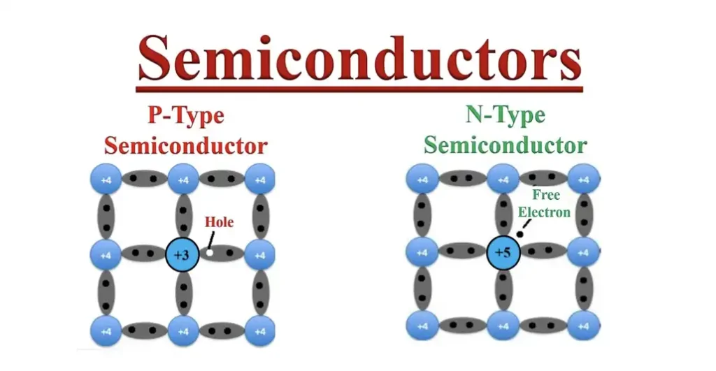
N-type semiconductors are created by doping an intrinsic semiconductor material, such as silicon or germanium, with group V elements like phosphorus, arsenic, or antimony. These impurities have one more valence electron than the semiconductor material, resulting in an excess of free electrons.
In an n-type semiconductor, the free electrons become the majority charge carriers, responsible for the flow of electric current. This abundance of negatively charged electrons gives n-type semiconductors their distinctive properties:
- Higher Electrical Conductivity: The high concentration of free electrons allows n-type semiconductors to have a higher electrical conductivity compared to their intrinsic counterparts.
- Current Flow Direction: In n-type semiconductors, the current flow is primarily due to the movement of electrons.
- Applications: N-type semiconductors are commonly used in devices that require high electron mobility, such as field-effect transistors (FETs) and microwave devices.
P-Type Semiconductors: Holes Take the Lead
In contrast, p-type semiconductors are created by doping an intrinsic semiconductor material with group III elements like boron, aluminum, or gallium. These impurities have one less valence electron than the semiconductor material, resulting in a surplus of “holes” – the absence of electrons.
In a p-type semiconductor, the holes become the majority charge carriers, responsible for the flow of electric current. This abundance of positively charged holes gives p-type semiconductors their unique characteristics:
- Lower Electrical Conductivity: Compared to n-type semiconductors, p-type semiconductors have a lower electrical conductivity due to the lower mobility of holes.
- Current Flow Direction: In p-type semiconductors, the current flow is primarily due to the movement of holes.
- Applications: P-type semiconductors are commonly used in devices that require high hole mobility, such as bipolar junction transistors (BJTs) and photodetectors.
N Type vs P Type Semiconductor
N-type and p-type semiconductors are the two fundamental building blocks of modern electronics. They are created by doping, which is the process of adding impurities to a pure semiconductor material (intrinsic semiconductor). This doping process alters the electrical properties of the material, making it easier to conduct electricity.
| Characteristic | N-Type Semiconductor | P-Type Semiconductor |
|---|---|---|
| Majority Charge Carriers | Electrons | Holes |
| Doping Impurities | Pentavalent (e.g., phosphorus, arsenic, antimony) | Trivalent (e.g., boron, aluminum, gallium) |
| Charge Carrier Concentration | High concentration of free electrons | High concentration of holes |
| Electrical Conductivity | High | Low |
| Applications | Diodes, transistors, integrated circuits | Used in conjunction with N-type semiconductors to create semiconductor devices |
Here’s a breakdown of the key differences between n-type and p-type semiconductors:
Majority Charge Carriers:
- N-type (negative): Has an excess of electrons. These extra electrons are the majority carriers of electrical current in n-type semiconductors. The dopant atoms used in n-type semiconductors typically have five valence electrons, contributing one extra electron for conduction. Examples of dopants for n-type include phosphorus (P) and arsenic (As).
- P-type (positive): Has an excess of “holes”. Holes are the absence of an electron in the valence band and act like positively charged particles. Holes are the majority carriers of electrical current in p-type semiconductors. The dopant atoms used in p-type semiconductors typically have three valence electrons, creating one “hole” for conduction. Examples of dopants for p-type include boron (B) and aluminum (Al).
Analogy:
Think of n-type semiconductors as having extra balls (electrons) in a game, and p-type semiconductors having empty spaces (holes) where balls should be. In both cases, these imbalances allow for easier flow within the material.
The Importance of the PN Junction:
The real magic happens when you combine n-type and p-type semiconductors together, forming a p-n junction. This creates a depletion zone where electrical properties are different, and it’s the foundation for various electronic devices like transistors and diodes.
The Power of the PN Junction
When an n-type semiconductor and a p-type semiconductor are joined together, they form a PN junction – the fundamental building block of many electronic devices, including diodes and transistors. The unique properties of the PN junction, such as the depletion region and the ability to control the flow of current, enable the creation of a wide range of electronic circuits and systems.
Conclusion: Harnessing the Differences
The distinct characteristics of n-type and p-type semiconductors are the foundation upon which the modern electronics industry has been built. By understanding and harnessing the unique properties of these semiconductor types, engineers and researchers have been able to develop increasingly sophisticated and innovative electronic devices, driving the technological progress that has transformed our world.
As the semiconductor industry continues to evolve, the interplay between n-type and p-type semiconductors will undoubtedly remain a crucial aspect of electronic design and innovation.