This comprehensive guide delves into the captivating realm of IC wafers. We’ll explore the intricate processes that bring these wafers to life, from the raw material to the cutting-edge fabrication techniques. We’ll unveil the secrets behind how billions of transistors and other circuits are meticulously etched onto their surface, forming the foundation of modern electronics.
Whether you’re a seasoned engineer, a curious tech enthusiast, or simply someone who wants to understand the invisible building blocks of our digital age, this guide is your roadmap to unlocking the mysteries of the IC wafer.
Let’s dive in
What Is Integrated Circuit Wafer
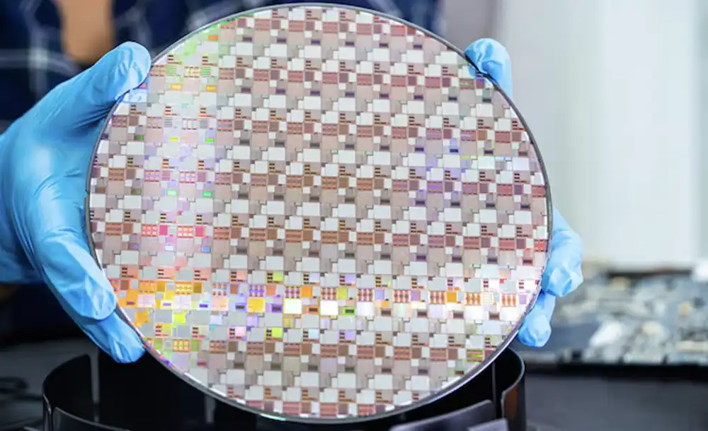
An integrated circuit (IC) wafer is a thin slice of semiconductor material, typically silicon, used in the fabrication of integrated circuits and other microdevices. The wafer serves as the substrate on which microelectronic devices are built through a series of processes that involve the deposition, patterning, and etching of various materials.
Key Aspects of Integrated Circuit Wafers:
- Material: Most IC wafers are made of silicon, although other materials such as gallium arsenide are also used for specific applications. Silicon is favored due to its excellent electrical properties and abundance.
- Size: Wafers come in various diameters, commonly ranging from 150 mm (6 inches) to 300 mm (12 inches). Larger wafers are more economical for mass production as they allow more ICs to be fabricated simultaneously.
Integrated Circuit Wafer Manufacturing Process
The manufacturing process of an integrated circuit (IC) wafer involves several intricate steps, each requiring precise control and advanced technology. Here’s a detailed overview of the main stages:
1. Crystal Growth
- Raw Material: High-purity silicon, derived from quartz, is the primary raw material.
- Czochralski Process: A seed crystal is dipped into molten silicon and slowly withdrawn, forming a cylindrical single crystal called an ingot.
2. Wafer Slicing
- Ingot Preparation: The ingot is precisely ground to a uniform diameter and sometimes doped with other elements to modify its electrical properties.
- Slicing: A diamond saw slices the ingot into thin wafers, typically 0.5-1 mm thick.
3. Wafer Polishing
- Lapping and Polishing: Wafers are lapped to remove saw marks and then polished to achieve a smooth, mirror-like surface. This ensures minimal surface defects.
4. Oxidation
- Thermal Oxidation: Wafers are heated in an oxygen-rich environment to grow a thin layer of silicon dioxide (SiO₂) on the surface. This layer acts as an insulator and protects the silicon.
5. Photolithography
- Photoresist Application: A light-sensitive photoresist layer is applied to the wafer.
- Mask Alignment: A photomask with the desired circuit pattern is aligned over the wafer.
- Exposure: Ultraviolet light exposes the photoresist through the mask, transferring the pattern onto the wafer.
- Developing: The exposed photoresist is developed, leaving a patterned resist layer on the wafer.
6. Etching
- Dry Etching: Uses plasma to remove material from the exposed areas, offering precise control.
- Wet Etching: Uses chemical solutions to dissolve exposed material. It’s less precise but faster for some applications.
7. Doping
- Ion Implantation: Ions of dopants are accelerated and embedded into the silicon to change its electrical properties.
- Diffusion: Wafers are heated to diffuse dopants into the silicon, forming regions of different conductivity.
8. Layer Deposition
- Chemical Vapor Deposition (CVD): A thin layer of material is deposited onto the wafer surface from a gas-phase reaction.
- Physical Vapor Deposition (PVD): Materials are physically sputtered or evaporated onto the wafer.
9. Metallization
- Metal Layer Deposition: Metal layers, typically aluminum or copper, are deposited to form electrical connections.
- Patterning: Photolithography and etching are used to define the metal interconnects.
10. Chemical-Mechanical Planarization (CMP)
- Planarization: Wafers undergo CMP to ensure a flat and even surface, crucial for multi-layer device structures.
11. Final Testing
- Probe Testing: Electrical tests are conducted on each die to identify defects.
- Inspection: Optical and electron microscopy are used to detect physical defects.
12. Dicing
- Sawing: The wafer is diced into individual chips or dies using a diamond saw.
13. Packaging
- Die Bonding: Individual dies are attached to a package or substrate.
- Wire Bonding: Fine wires connect the die to the package leads.
- Encapsulation: The assembly is encased in a protective material.
14. Final Testing and Quality Control
- Electrical Testing: Packaged ICs undergo rigorous testing to ensure functionality.
- Burn-In Testing: ICs are tested under high-stress conditions to identify early failures.
15. Shipment
- Sorting and Packaging: Fully tested and qualified ICs are sorted, packaged, and shipped to customers.
Each of these steps is crucial for producing high-quality, reliable integrated circuits used in a multitude of electronic devices. The entire process requires cleanroom environments, advanced equipment, and meticulous quality control to achieve the precision necessary for modern electronics.
Integrated Circuit Wafer Applications
Integrated circuit (IC) wafers are fundamental to the operation of a wide array of electronic devices and systems. Here are some key applications:
1. Consumer Electronics
- Smartphones and Tablets: IC wafers are used to manufacture processors, memory chips, and various sensors that power mobile devices.
- Laptops and Computers: Central processing units (CPUs), graphics processing units (GPUs), and memory modules are all fabricated from IC wafers.
- Wearables: Devices like smartwatches and fitness trackers rely on IC wafers for their compact and efficient electronics.
2. Automotive Industry
- Engine Control Units (ECUs): IC wafers are used in the microcontrollers and sensors that manage engine functions.
- Advanced Driver Assistance Systems (ADAS): These systems use ICs for functions like collision detection, lane departure warnings, and adaptive cruise control.
- Infotainment Systems: ICs drive the multimedia and connectivity features in modern vehicles.
3. Industrial Applications
- Automation and Robotics: IC wafers are used in the controllers and sensors that power industrial robots and automated systems.
- IoT Devices: Industrial Internet of Things (IIoT) devices use ICs for monitoring and controlling various industrial processes.
4. Healthcare and Medical Devices
- Diagnostic Equipment: ICs are used in medical imaging devices like MRI and CT scanners.
- Wearable Health Monitors: Devices that monitor heart rate, blood pressure, and other vital signs rely on ICs.
- Implantable Devices: Pacemakers and other implantable medical devices use ICs for their critical functions.
5. Telecommunications
- Networking Equipment: Routers, switches, and other networking hardware use ICs to manage data transmission and routing.
- Mobile Communication: Base stations and other infrastructure for mobile networks depend on ICs.
6. Aerospace and Defense
- Navigation Systems: ICs are used in GPS and other navigation systems.
- Avionics: Aircraft control systems, communication systems, and instrumentation use ICs for reliable performance.
- Defense Electronics: ICs are used in radar systems, missile guidance, and other defense technologies.
7. Renewable Energy
- Solar Power Systems: ICs are used in the control systems of solar panels and inverters.
- Wind Turbines: Control and monitoring systems in wind turbines use ICs to optimize performance.
8. Entertainment Systems
- Gaming Consoles: The processors and graphics chips in gaming consoles are manufactured from IC wafers.
- Home Theaters: Audio and video processing in home theater systems rely on ICs.
9. Data Centers and Cloud Computing
- Servers: High-performance processors and memory ICs are crucial for data center operations.
- Storage Solutions: Solid-state drives (SSDs) and other storage technologies use ICs for data storage and retrieval.
10. Smart Home Devices
- Home Automation: ICs are used in smart thermostats, lighting systems, and security devices.
- Voice Assistants: Devices like smart speakers rely on ICs for processing voice commands and connecting to other smart devices.
11. Scientific Research
- Laboratory Equipment: Advanced research instruments like electron microscopes and spectrometers use ICs for data processing and control.
- Particle Accelerators: ICs are used in the control systems of particle accelerators and other large-scale scientific apparatus.
Conclusion
Integrated circuit (IC) wafers form the bedrock of modern electronic technology, underpinning the vast array of devices and systems that drive today’s digital world. From the raw materials and intricate manufacturing processes to their diverse applications across various industries, IC wafers demonstrate remarkable versatility and critical importance.
In consumer electronics, IC wafers enable the development of high-performance smartphones, computers, and wearable devices. The automotive industry relies on them for advanced driver assistance systems and infotainment, enhancing safety and user experience. Industrial automation, healthcare, telecommunications, aerospace, defense, renewable energy, and data centers all depend on the precise and reliable functionality provided by IC wafers.