In 2024, understanding Integrated Circuit Substrate is paramount for advancing electronic technologies. This comprehensive guide explores the pivotal role of Integrated Circuit Substrate in modern electronics, delving into its materials, applications, and emerging trends.
From foundational principles to cutting-edge innovations, this resource aims to equip readers with essential knowledge to navigate the evolving landscape of electronic substrate technologies.
What Is Integrated Circuit Substrate?
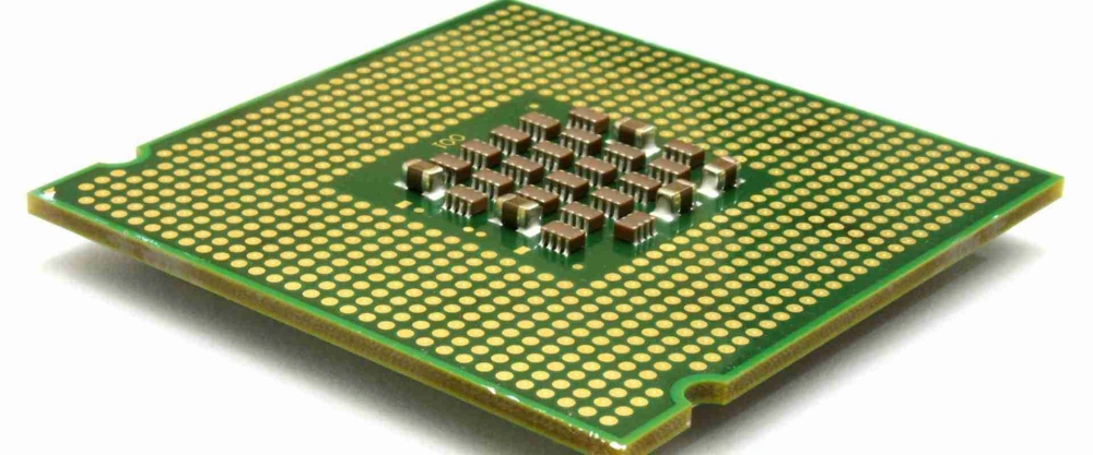
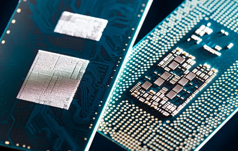
The foundation of IC packages is the integrated circuit substrate, also known as IC package substrate. These substrates protect the IC while facilitating connections between the IC and the PCB’s trace network, significantly influencing circuit performance.
They consist of multiple layers with a central supporting core. Additionally, IC substrates feature a network of drill holes and conductor pads that are often more densely packed than those found in traditional PCBs, making their fabrication challenging.
Why Integrated Circuit Substrate Is Important?
The integrated circuit substrate is crucial for your electronics. It provides structural support and electrical connections for components, ensuring they function reliably. Without it, devices couldn’t communicate effectively or manage heat, risking failures. It’s the backbone that keeps your electronics running smoothly.
Features Of Integrated Circuit Substrate
Miniaturized Circuit
The substrate provides a stable foundation for mounting electronic components such as transistors, resistors, and capacitors. This enables engineers to densely pack intricate circuitry into smaller spaces, crucial for the development of compact and portable devices like smartphones, tablets, and wearable technology.
Miniaturization allows for enhanced functionality without compromising on performance, meeting the growing demand for smaller, lighter electronics.
Cost-effectiveness
By optimizing material usage and manufacturing processes, the Integrated Circuit Substrate contributes to cost-effectiveness in electronics production. It helps reduce overall production costs while maintaining high-quality standards. Manufacturers can efficiently utilize resources, minimize waste, and streamline assembly processes, resulting in competitively priced electronic products that appeal to a broad consumer base.
Reliability
Serving as a robust platform, the substrate ensures reliable performance of electronic devices. It provides mechanical support and secure electrical connections between components, safeguarding against physical damage and environmental stresses. This reliability is crucial for maintaining consistent operation over extended periods, enhancing user satisfaction and reducing maintenance and repair costs.
Lower Failure Rates
The substrate’s design and material properties play a critical role in minimizing failure rates within electronic devices. By offering a secure mounting platform and stable electrical pathways, it reduces the risk of connectivity issues, short circuits, and other electrical faults. Additionally, the substrate’s resilience to thermal fluctuations and mechanical stresses helps mitigate the potential for component failure, ensuring robust performance and longevity.
High Efficiency And Energy Savings
Efficient heat dissipation and electrical performance optimization are key attributes of the Integrated Circuit Substrate. It effectively manages heat generated by active components, preventing overheating and maintaining optimal operating conditions.
By reducing energy consumption associated with cooling mechanisms, the substrate promotes energy efficiency in electronic devices. This not only enhances environmental sustainability but also extends battery life and improves overall device efficiency, meeting the demands for greener technology solutions.
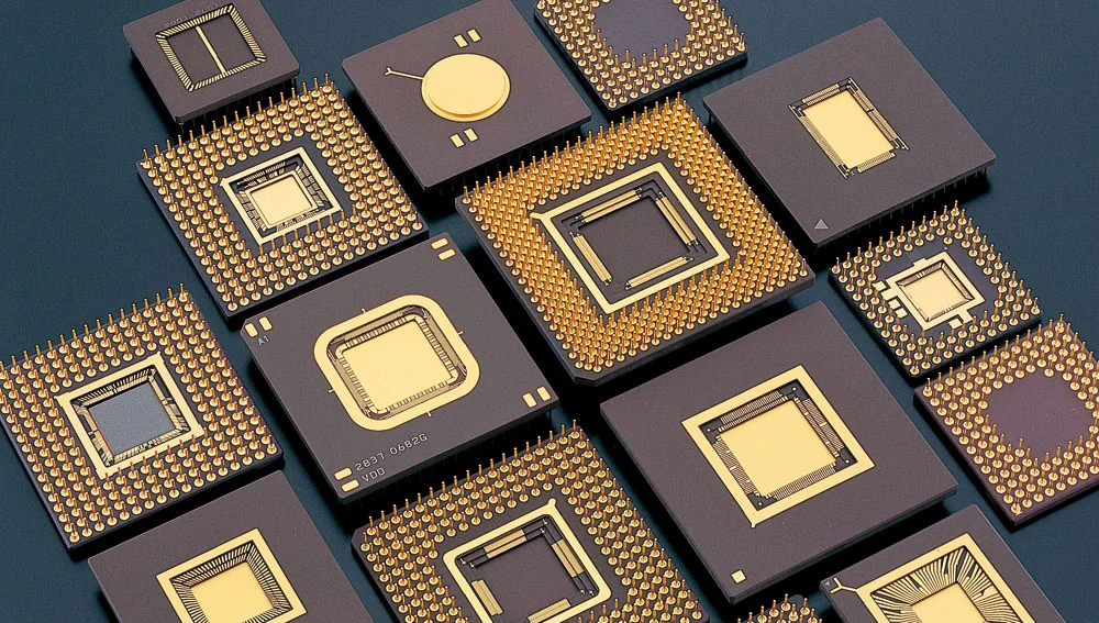
Classification Of Integrated Circuit Substrate
Integrated Circuit Substrate encompass a wide variety and are categorized broadly into three types: package type, packaging style, bonding technology, and material properties. Additionally, they can be further classified based on their specific application fields.
Packaging Type Classification
Ball Grid Array IC Substrate: Ball Grid Array (BGA) IC substrates feature a grid of solder balls underneath the chip, enhancing electrical connections and thermal dissipation. Ideal for compact designs, BGAs support high pin counts and robust performance in demanding applications.
Chip-Scale Package IC Substrate: Chip-Scale Package (CSP) IC substrates offer a compact form factor where the package size closely matches the chip size. These substrates minimize footprint, making them suitable for portable devices. CSPs ensure efficient heat management and reliable electrical connections, essential for modern integrated circuits.
Flip-Chip IC Substrate: Flip-Chip IC substrates enable direct connection of the chip to the substrate, enhancing performance by shortening signal paths. This design reduces interconnect inductance, enhancing speed and reliability in high-frequency applications. Flip-chip substrates support miniaturization and efficient thermal management, crucial in advanced electronics.
Classification By Material Characteristics
Multi-Chip Module IC Substrate: Multi-Chip Module (MCM) IC substrates integrate multiple chips on a single substrate, optimizing space and performance. They facilitate complex system integration, enhancing efficiency in high-density applications like servers and telecommunications equipment.
Rigid IC Substrate: Rigid IC substrates are made from inflexible materials like fiberglass-reinforced epoxy (FR-4) or other rigid laminates. They provide stable support for components, ensuring precise alignment and reliable electrical connections in standard electronic devices and PCB assemblies.
Flexible IC Substrate: Flexible IC substrates use flexible materials such as polyimide, allowing for bending and conforming to non-planar surfaces. They are crucial in applications requiring lightweight and compact designs, such as wearable electronics and flexible displays.
Ceramic IC Substrate: Ceramic IC substrates utilize ceramic materials like alumina or aluminum nitride, offering excellent thermal conductivity and mechanical stability. They are preferred for high-power and high-frequency applications where heat dissipation and reliability are paramount, such as RF amplifiers and power modules.
Classification By Bonding Technology
Wire Bonding: Wire bonding is a traditional method where thin wires connect the chip to the substrate, typically using gold or aluminum wires. It’s versatile for various chip sizes and widely used in consumer electronics. Wire bonding allows for easy repair and modification but may limit performance in high-frequency applications due to inductance.
Flip Chip (FC): Flip Chip bonding involves directly mounting the chip upside-down on the substrate, with solder bumps connecting them. This method minimizes interconnect length, reducing parasitic capacitance and inductance, enhancing performance in high-speed and high-frequency applications like CPUs and GPUs. FC bonding supports miniaturization and improves thermal management.
Tape Automated Bonding (TAB): Tape Automated Bonding (TAB) uses a flexible tape with pre-formed leads to connect the chip to the substrate. It’s efficient for mass production of small, lightweight devices like LCDs and sensors. TAB offers precise alignment and high reliability but requires specialized equipment and may be less suitable for high-power applications due to thermal limitations.
Manufacturing Methods Of Integrated Circuit Substrate
To begin with, understanding the three distinct PCB manufacturing processes is crucial. Currently, there are three types: subtractive process (SP), additive process (AP), and modified semi-additive process (MSAP).
Subtractive Process (SP)
This traditional PCB manufacturing method begins by plating a copper layer onto copper-clad laminate, applying a protective dry film over the circuit and through-holes, and subsequently etching away excess copper. A notable drawback is lateral etching during this process, limiting minimum line width/spacing to over 50 µm (2 mils), suitable mainly for standard PCBs, FPCs, and HDI PCB products.
Additive Process (AP)
In this method, a photosensitive catalyst on an insulating substrate is exposed to the circuit, followed by selective chemical deposition of thick copper where exposed, forming a complete PCB. This approach avoids lateral etching, achieving high precision with line widths/spacings below 20 µm.
However, it demands advanced substrates and process flows, resulting in high costs and lower output, primarily used for WB or FC IC substrates with process capabilities up to 12 µm/12 µm.
Modified Semi-Additive Process (MSAP)
Initially, a thin copper layer is electroplated onto the copper-clad laminate. Areas not needing protection are selectively removed by flash etching, leaving the required copper lines. Since the initial copper layer is thin, flash etching minimally affects the edges.
MSAP offers high yield and lower production costs compared to SP and AP methods, making it the preferred choice for fine circuit board manufacturing. Widely adopted for CSP, WB, and FC IC substrates, and fine-line boards like SLPs, which require minimum line width/spacings of 30 µm/30 µm, necessitating MSAP technology.
Production Technologies Of Integrated Circuit Substrate
Digital Imaging Systems
These systems handle challenging applications like Ball Grid Array/Chip Scale Package (BGA/CSP), Flip-Chip Chip-Scale Package (FCCSP), and Flip-Chip Ball Grid Array (FCBGA). They not only reduce Total Cost of Ownership (TCO) but also enhance manufacturing yields.
Automated Optical Inspection Systems
Automated optical inspection systems offer high-resolution, high-throughput inspection of IC substrates such as FCCSP and FCBGA. Using single-scan technology, they capture multiple light sources during substrate panel inspection.
Ultraviolet Laser Drilling Systems
Ultraviolet laser drilling systems feature a fine diameter of 20 µm, superior accuracy of 6 µm, and excellent beam quality. They support advanced packaging applications like Low-Temperature Co-Fired Ceramic (LTCC), organic interposers, and embedded devices. Additive printing systems are designed to print dams for System in Package (SiP), BGA, and FCCSP modules.
Automated Optical Shaping Systems (AOS)
Automated optical shaping systems specialize in shaping fine-panel or complex defects in cutting-edge IC substrates such as FCCSP and FCBGA. This reduces scrap and enables substrate manufacturers to increase yield effectively.
What Is Integrated Circuit Substrate Used For?
Memory Chip Packaging
Integrated Circuit Substrate PCBs are crucial for memory chip packaging, ensuring precise electrical connections and compact form factors in devices like smartphones, laptops, and tablets. They optimize data storage and retrieval speed, enhancing device performance.
Micro-electromechanical Systems (MEMS) Chip Packaging
For MEMS devices, Integrated Circuit Substrate PCBs provide robust structural support and reliable electrical pathways. They enable intricate sensor and actuator integration in applications ranging from consumer electronics to medical devices, ensuring accurate and sensitive performance.
Radiofrequency (RF) Chip Packages
Integrated Circuit Substrate PCBs play a vital role in RF chip packages by providing low-loss transmission lines and efficient heat dissipation. They support high-frequency operations essential for wireless communication devices like smartphones and base stations, ensuring reliable signal transmission.
Processor Chip Packaging
Essential for high-performance computing, Integrated Circuit Substrate PCBs facilitate processor chip packaging with optimized power delivery and thermal management. They enable complex computational tasks in laptops, printers, and memory devices like RAM modules, enhancing overall system speed and efficiency.
Integrated Circuitry In High-Speed Communication Devices
Integrated circuit substrate PCBs integrate complex circuitry for high-speed communication devices, ensuring stable signal processing and transmission. Found in smartphones, laptops, and tablets, they support seamless connectivity and data exchange in modern digital environments.
Conclusion
In conclusion, the field of Integrated Circuit Substrate continues to evolve as technology advances. From memory chip packaging to high-speed communication devices, IC substrates play a critical role in supporting and enhancing the performance of electronic components.
As we move forward in 2024, their application in diverse industries like telecommunications, automotive, and medical care underscores their indispensability in modern electronics. Embracing innovative materials and manufacturing processes ensures IC substrates remain at the forefront of technological innovation, driving efficiency and reliability in electronic devices worldwide.