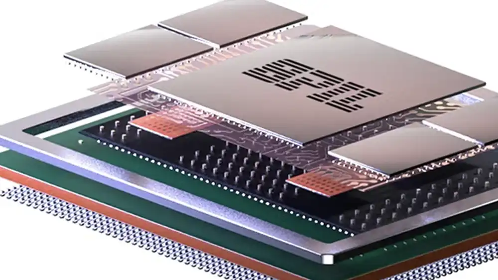
Integrated circuit (IC) packaging is a crucial aspect of modern electronics, encapsulating semiconductor devices to protect them and enable their integration into electronic systems. The development of IC packaging has evolved significantly, impacting the functionality, size, and performance of electronic devices.
This article delves into the various types of IC packages, their technical specifications, applications, benefits, challenges, and future prospects.
What Is Integrated Circuit (IC) Packaging
Integrated Circuit (IC) packaging is an essential process in electronics, ensuring the protection, connectivity, and functionality of semiconductor devices.
This process has evolved from simple methods to highly sophisticated techniques, significantly impacting the size, performance, and cost of electronic devices. In this article, we will explore the various types of IC packages, their applications, benefits, challenges, and future trends.
Technical Specifications of Integrated Circuit Packaging
Definition and Purpose of IC Packaging
IC packaging serves to encase semiconductor chips, providing physical protection and facilitating electrical connections to a printed circuit board (PCB). This packaging ensures the chip’s durability, aids in heat dissipation, and protects it from environmental factors such as moisture and contaminants.
Materials Used in IC Packaging
The materials used in IC packaging include:
- Ceramics: Known for their excellent thermal and electrical properties, ceramics are often used in high-performance and high-reliability applications.
- Plastics: Widely used due to their cost-effectiveness and versatility, plastics are common in consumer electronics.
- Metals: Used for lead frames and connections due to their good electrical conductivity and mechanical strength.
Manufacturing Processes
The manufacturing processes for IC packaging involve several steps, including:
- Wafer Dicing: Cutting the wafer into individual chips.
- Die Attachment: Attaching the die to a substrate or lead frame.
- Wire Bonding: Connecting the die to the lead frame or substrate using fine wires.
- Encapsulation: Enclosing the die and wires in protective materials.
- Testing: Ensuring the functionality and reliability of the packaged IC.
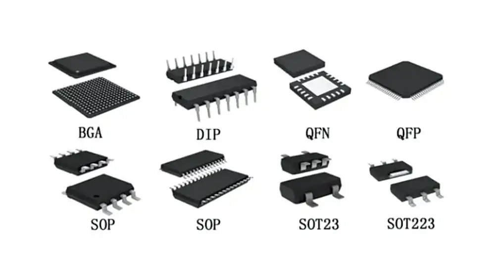
Types of Integrated Circuit Packaging
Here are some widely used integrate circuit packaging in the following:
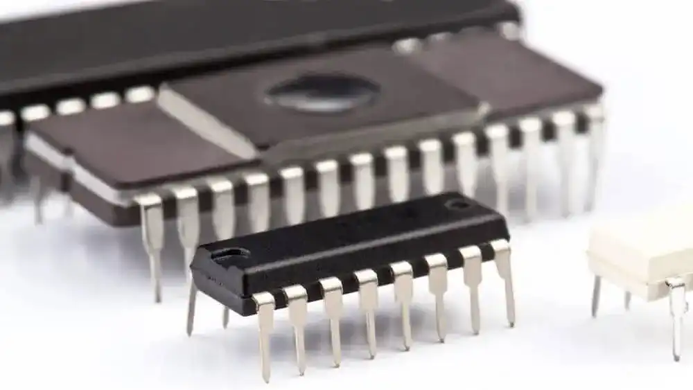
Dual In-line Package (DIP)
A traditional and widely used package, the Dual In-line Package (DIP) features two parallel rows of pins. These packages are easy to handle and suitable for through-hole mounting on PCBs.
Surface-Mount Device (SMD)
Surface-Mount Devices (SMDs) are designed for surface mounting, allowing components to be placed directly onto the surface of the PCB. This method reduces space and enhances performance.
Chip-on-Board (COB)
In the Chip-on-Board (COB) approach, the semiconductor die is mounted directly onto the PCB and then encapsulated. This method improves thermal performance and reduces manufacturing costs.
Ball Grid Array (BGA)
The Ball Grid Array (BGA) package uses a grid of solder balls on the bottom of the package for connections. This design provides excellent thermal and electrical performance and is ideal for high-density applications.
Chip Scale Package (CSP)
A Chip Scale Package (CSP) is almost the same size as the die itself, offering a compact and efficient solution for space-constrained applications.
Quad Flat Package (QFP)
The Quad Flat Package (QFP) has leads on all four sides, making it suitable for applications requiring high pin counts. It provides a balance between performance and cost.
Pin Grid Array (PGA)
The Pin Grid Array (PGA) features an array of pins on the bottom surface. It is often used in microprocessors and other high-performance applications due to its reliable electrical connections.
Wafer-Level Package (WLP)
Wafer-Level Packaging (WLP) involves packaging the die at the wafer level, allowing for a smaller footprint and improved performance. This technique is increasingly popular in mobile and wearable devices.
System-in-Package (SiP)
System-in-Package (SiP) integrates multiple dies into a single package, offering a complete solution with reduced size and improved performance. It is commonly used in complex, multifunctional devices.
Flip-Chip Package
The Flip-Chip Package involves flipping the die and connecting it directly to the substrate using solder bumps. This method provides superior electrical performance and thermal management.
Applications of IC Packages
Consumer Electronics
IC packages are integral to consumer electronics, including smartphones, tablets, laptops, and gaming consoles. They enable miniaturization and enhance device performance.
Automotive Industry
In the automotive industry, IC packages are used in engine control units, infotainment systems, and advanced driver-assistance systems (ADAS), contributing to vehicle safety and efficiency.
Medical Devices
IC packaging plays a vital role in medical devices, such as pacemakers, diagnostic equipment, and wearable health monitors, ensuring reliability and longevity.
Telecommunications
Telecommunications equipment, including routers, modems, and base stations, relies on IC packages for efficient data processing and transmission.
Industrial Applications
In industrial settings, IC packages are used in automation systems, sensors, and control units, enhancing productivity and operational efficiency.
Benefits of Various IC Packages
Miniaturization
IC packaging allows for the miniaturization of electronic devices, enabling the creation of compact and portable gadgets.
Enhanced Performance
Advanced packaging techniques improve the performance of electronic devices by enhancing electrical and thermal characteristics.
Cost Efficiency
Many IC packaging methods are cost-effective, making them suitable for mass production and reducing the overall cost of electronic products.
Improved Heat Dissipation
Effective IC packaging ensures efficient heat dissipation, which is crucial for maintaining the performance and longevity of electronic components.
Reliability and Durability
Proper IC packaging protects semiconductor devices from environmental damage, ensuring reliability and durability in various applications.
Latest Innovations in IC Packaging
Advanced Packaging Technologies
New technologies, such as fan-out wafer-level packaging (FOWLP) and embedded die packaging, are revolutionizing the industry by offering enhanced performance and miniaturization.
3D IC Packaging
3D IC packaging involves stacking multiple dies vertically, reducing space and improving performance. This innovation is particularly significant in high-performance computing and data centers.
Heterogeneous Integration
Heterogeneous integration combines different types of components, such as analog and digital, into a single package, enhancing functionality and performance.
Comparing Different IC Packages
Each IC package type has its unique advantages and disadvantages. For instance, while DIP packages are easy to handle, BGA packages offer superior performance and miniaturization.
Pros and Cons of Each Type
- DIP: Easy to handle, but limited in pin count and performance.
- SMD: Excellent for miniaturization and performance, but requires precise manufacturing.
- COB: Cost-effective and good for thermal management, but limited to specific applications.
- BGA: High performance and density, but more complex and expensive to manufacture.
- CSP: Very compact and efficient, but can be more challenging to assemble.
- QFP: Good balance of cost and performance, but limited in thermal dissipation.
- PGA: Reliable electrical connections, but takes up more space.
- WLP: Small footprint and good performance, but higher manufacturing complexity.
- SiP: Integrates multiple functions in a single package, but can be more costly.
- Flip-Chip: Superior electrical and thermal performance, but requires advanced manufacturing techniques.
How to Select Integrated Circuit Packaging
Selecting the right IC package involves considering several factors:
- Application Requirements: Determine the specific requirements of your application, including performance, size, and environmental conditions.
- Thermal Management: Evaluate the thermal performance needs and choose a package that can effectively dissipate heat.
- Cost Constraints: Balance the cost of the IC package with your budget constraints, considering both manufacturing and long-term operational costs.
- Manufacturing Capabilities: Ensure that your manufacturing process can accommodate the selected package type.
- Reliability: Consider the reliability and longevity of the package in the intended application environment.
- Pin Count and Density: Choose a package that meets the pin count and density requirements of your design.
Best Practices for Implementing IC Packages
- Design for Manufacturability: Ensure that your PCB design accommodates the selected IC package, with appropriate pad layouts and clearances.
- Thermal Management: Incorporate thermal vias, heat sinks, or other cooling solutions to manage heat dissipation.
- Signal Integrity: Design with proper trace routing, impedance matching, and decoupling capacitors to maintain signal integrity.
- Testing and Quality Control: Implement rigorous testing and quality control measures to ensure reliability and performance.
- Documentation: Maintain detailed documentation of your design and manufacturing process to facilitate troubleshooting and future upgrades.
Conclusion
Integrated circuit packaging is a fundamental aspect of modern electronics, enabling the protection, connectivity, and performance of semiconductor devices. From traditional DIP packages to advanced 3D and heterogeneous integration techniques, the evolution of IC packaging continues to drive innovation in various industries. Understanding the different types of IC packages, their benefits, challenges, and future trends is essential for engineers, designers, and manufacturers aiming to create efficient, reliable, and cost-effective electronic products.
As the electronics industry advances, the importance of selecting and implementing the appropriate IC packaging technology cannot be overstated. Future trends in flexible, stretchable, and high-performance packaging will open new possibilities, further enhancing the capabilities and applications of electronic devices.