The integrated circuit (IC) manufacturing process, also known as fabrication or fab, is a complex and precise series of steps that transforms raw silicon wafers into the tiny electronic brains that power our devices.
What Are Integrated Circuits
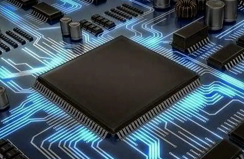
An integrated circuit (IC), also commonly called a microchip, computer chip, or simply chip, is a tiny electronic marvel. It’s essentially a miniaturized marvel of engineering, cramming billions of microscopic electronic components like transistors, resistors, capacitors, and more onto a single piece of silicon. Imagine a city built on a fingertip, with each building performing a specific electronic function and all connected by a network of microscopic streets. That’s kind of like an integrated circuit!
Here’s a breakdown of what makes ICs so important:
- Small Size & High Density: ICs can pack an incredible number of electronic components into a very small space. This miniaturization is crucial for developing compact and portable electronic devices.
- Powerhouse Performance: By integrating billions of components, ICs can perform complex calculations and functions at incredibly high speeds. This processing power fuels everything from smartphones and laptops to complex medical equipment and space probes.
- Versatility: ICs come in a wide variety of designs, each tailored to a specific purpose. They can be used for simple tasks like controlling a light switch or for highly complex operations like processing video or running artificial intelligence algorithms.
- Cost-Effectiveness: While the initial research and development for IC design can be expensive, the mass production of these chips makes them relatively inexpensive. This affordability allows for the widespread use of electronics in our daily lives.
Here are some real-world examples of ICs in action:
- The processor in your computer: This complex IC is the brain of your computer, responsible for executing instructions and managing all its operations.
- The memory chips in your phone: These ICs store data like photos, videos, and applications on your phone.
- The graphics card in your gaming console: This specialized IC handles the processing of visual information, creating the high-resolution graphics you see in games.
- The Wi-Fi chip in your tablet: This tiny IC allows your device to connect to wireless networks and access the internet.
Integrated circuits are the building blocks of modern electronics. Their miniaturization, performance, versatility, and affordability have revolutionized the way we live, work, and interact with the world around us.
Integrated Circuit Manufacturing Process
The journey of transforming a raw silicon wafer into a powerful integrated circuit involves a fascinating dance of precision and technology. Here’s a closer look at each step about how are integrated circuits manufactured
Step 1. Wafer Preparation:
- Starting Material: The foundation for any IC is a disc-shaped slice of ultra-pure silicon, typically 12-inches in diameter and incredibly thin (around the thickness of a human hair). This silicon undergoes a rigorous selection process to ensure it’s free of defects that could disrupt circuit function later.
- Cleaning & Polishing: Even the slightest imperfection on the wafer’s surface can compromise the delicate circuit patterns. To create a pristine canvas, the wafer undergoes a multi-step cleaning process using chemicals and deionized water. This is followed by polishing with special slurries to achieve a mirror-like surface.
Step 2. Oxidation:
Growing a Layer: A thin layer of silicon dioxide (SiO2) is grown on the wafer’s surface using a high-temperature chemical vapor deposition (CVD) process. This layer acts as a crucial insulator, preventing unwanted electrical currents from flowing between different parts of the circuit. It also serves as a base for further processing steps.
Step 3. Lithography:
- Creating the Pattern: This is like creating a blueprint for the circuit. A light-sensitive material called photoresist is coated onto the wafer. Then, a mask containing the intricate circuit design is placed on top. This mask acts like a stencil, allowing precisely controlled light to reach certain areas of the photoresist when exposed to a light source (typically ultraviolet light).
- Developing the Pattern: The wafer is then submerged in a developer solution. This solution selectively removes the exposed (or unexposed) photoresist depending on the type of resist used. This creates a positive or negative image of the circuit pattern etched onto the photoresist layer.
Step 4. Etching:
- Transferring the Pattern: Now comes the carving. Using a carefully chosen etching technique (chemical or plasma etching), the exposed silicon dioxide is selectively removed, effectively transferring the circuit pattern from the photoresist onto the underlying silicon surface. This etching process carves away unwanted areas, defining the intricate features of the circuit.
- Removing Photoresist: Once the etching is complete, the remaining photoresist is stripped away, leaving behind the etched circuit features on the silicon.
Step 5. Doping:
Introducing Impurities: While silicon is a fantastic semiconductor, it needs a little “help” to conduct electricity effectively. Doping introduces very precise amounts of specific impurities (typically elements like boron or phosphorus) into designated areas of the silicon. These impurities create regions with different electrical properties (p-type and n-type), which are essential building blocks for transistors, the fundamental elements of any integrated circuit.
Step 6. Deposition:
Adding Layers: Building a complex IC often requires multiple layers of interconnected components. This step involves depositing thin films of various materials onto the wafer’s surface using techniques like physical vapor deposition (PVD) or chemical vapor deposition (CVD). These deposited materials can be conductors like aluminum (for interconnections between circuit elements), insulators like silicon dioxide (for further isolation), or even other semiconductors for specialized functions.
Step 7. Patterning Again (Steps 3-6 Repeated):
The magic of IC fabrication lies in its ability to create complex structures. Steps 3-6 (lithography, etching, doping, deposition) are often repeated multiple times, building layer upon layer of interconnected circuits. Each layer adds new functionality to the overall chip. Advanced ICs can have dozens of these intricately patterned layers.
Step 8. Testing and Inspection:
Quality Control: Throughout the process, rigorous quality control checks are performed. Electrical tests ensure the circuits are functioning as designed and identify any defective areas. Microscopic inspections are also conducted to detect physical imperfections. Any wafers with defects are discarded to maintain the high yield and quality of the final product.
Step 9. Dicing:
Separating Circuits: After successful testing and inspection, the wafer is transformed from a single intricate circuit layout into hundreds or even thousands of individual integrated circuits. A specialized dicing saw precisely cuts the wafer into tiny squares, each containing a single IC chip.
Step 10. Packaging:
Protection and Connection: The individual chips are incredibly fragile and need protection from the environment and a way to connect to other components. They are mounted onto a package, typically made of ceramic or plastic. This package provides physical protection, electrical connections through tiny wires or bond pads, and a way to dissipate heat generated by the chip during operation.
Step 11. Final Testing
Last Check: The packaged ICs undergo a final round of rigorous electrical testing to ensure they meet all performance specifications and functionality requirements. This testing identifies any defective chips that may have slipped through earlier checks. Only ICs that pass these final tests are deemed functional and ready for shipment to device manufacturers.
Beyond the Basics:
This explanation covers the fundamental steps in IC manufacturing. However, the world of chip fabrication is constantly evolving with even more sophisticated techniques:
- Photolithography Advancements: Extreme ultraviolet (EUV) lithography pushes the resolution limits, allowing for even smaller and more intricate circuit features.
- 3D Integration: Stacking multiple layers of transistors vertically (instead of just horizontally) creates 3D ICs that offer increased functionality and performance in a smaller footprint.
- Nanotechnology: As technology miniaturizes, nanomaterials and processes play an increasingly important role in chip fabrication.
The Importance of IC Manufacturing:
The complex and precise world of IC manufacturing is the foundation for modern electronics. From the smartphones in our pockets to the computers on our desks, these tiny integrated circuits power the technological advancements that shape our lives.
Conclusion
The journey from a raw silicon wafer to the tiny powerhouse chip powering your phone is a fascinating dance of precision and technology. The integrated circuit (IC) manufacturing process, a marvel of modern engineering, crams billions of microscopic components onto a single chip, enabling the incredible functionality of modern electronics.
This complex process, with steps like lithography, etching, doping, and deposition, pushes the boundaries of miniaturization and performance. The constant evolution of IC manufacturing, with advancements like extreme ultraviolet lithography and 3D integration, promises even smaller, faster, and more powerful chips in the future.
The world of IC manufacturing is a cornerstone of technological progress. Whether you’re a student curious about how electronics work, an engineer pushing the boundaries of chip design, or simply someone who appreciates the power of technology in your pocket, understanding the IC manufacturing process offers a deeper appreciation for the tiny marvels that shape our world.
Here are some ways to delve deeper:
- Explore online resources and educational videos that showcase the IC manufacturing process in more detail.
- Research the companies and organizations at the forefront of chip design and fabrication.
- Consider a career path in engineering or related fields that contribute to the future of IC technology.
By understanding and appreciating the intricate world of IC manufacturing, we can better appreciate the technology that shapes our lives and fuels the innovations of tomorrow.