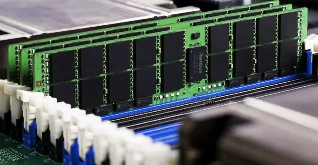
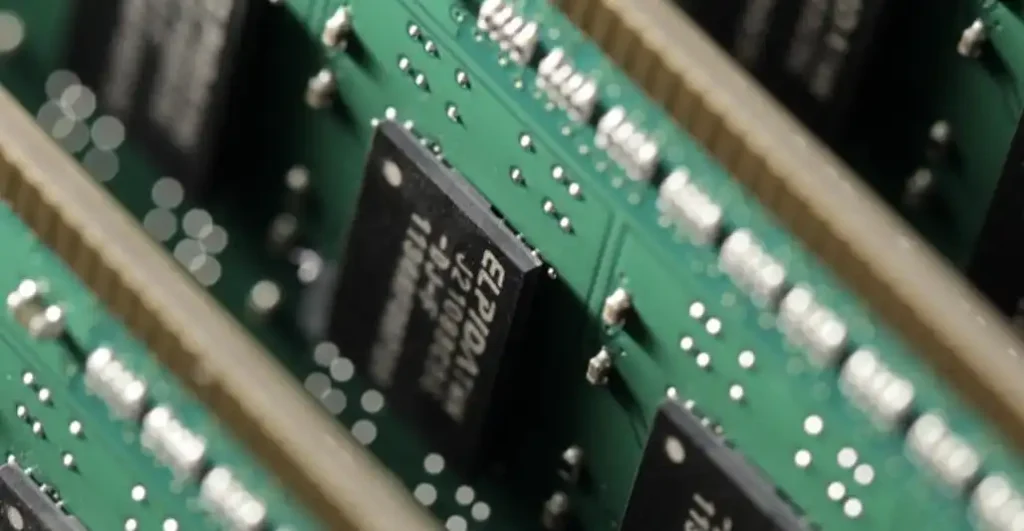
In today’s digital world, data reigns supreme. From the complex calculations on your computer to the high-resolution photos on your phone, everything relies on the invisible workhorses behind the scenes: memory chips. But how exactly do these tiny marvels store and retrieve information?
This comprehensive blog delves into the fascinating world of memory chips, exploring their intricate workings and the technologies that power them.
Memory Cells and Transistors
At the heart of every memory chip lies a fundamental unit called a memory cell. This microscopic circuit is responsible for storing a single bit of data, which is the foundation of all digital information. There are two main types of memory cells:
- DRAM Cells (Dynamic Random Access Memory): These cells utilize capacitors to hold data as electrical charge. However, DRAM is volatile, meaning it loses its data when the power is off. This makes DRAM ideal for storing frequently accessed information during computer operation.
- Flash Memory Cells: Unlike DRAM, flash memory cells employ transistors to trap electrons, enabling them to retain data even without power. This non-volatile property makes flash memory perfect for storing permanent data like files and programs.
Types of Memory Chips: Catering to Different Need

Let’s delve deeper into the types of memory chips, exploring their specific characteristics and applications:
1. Random Access Memory (RAM):
Dynamic Random-Access Memory (DRAM): As mentioned earlier, DRAM is the prevalent form of RAM, offering high speed and affordability. However, its volatile nature necessitates constant refreshing of data to prevent information loss. Here are some sub-categories of DRAM:
- SDRAM (Synchronous Dynamic RAM): Synchronizes its operations with the system clock for improved efficiency. Most computers today utilize DDR SDRAM (Double Data Rate SDRAM), which can transfer data twice per clock cycle.
- DDR SDRAM Variants (DDR2, DDR3, DDR4, DDR5): These represent successive generations of DDR SDRAM, each offering faster data transfer rates and lower power consumption compared to its predecessor.
- Static Random-Access Memory (SRAM): SRAM boasts significantly faster access times than DRAM but comes at a cost. It utilizes a more complex circuitry, making it more expensive and less dense (offering lower storage capacity per unit area). Due to these factors, SRAM is typically used in smaller capacities for critical tasks requiring high-speed data access, such as CPU cache memory.
2. Read-Only Memory (ROM):
- Masked ROM (MROM): This type of ROM has its data permanently etched during the manufacturing process. It’s cost-effective for mass production of devices with pre-programmed, unchanging data, like bootloaders in embedded systems.
- Programmable ROM (PROM): Unlike MROM, PROMs can be programmed once using a high-voltage electrical pulse. However, this process is irreversible, limiting their flexibility.
- Erasable Programmable ROM (EPROM): EPROMs offer more flexibility compared to PROMs. They can be erased using ultraviolet (UV) light and then reprogrammed, but the erasure process is slow and inconvenient.
- Electrically Erasable Programmable ROM (EEPROM): EEPROMs address the limitations of EPROMs by enabling erasure and reprogramming electrically. This allows for in-system updates and customization.
3. Flash Memory:
As the blog mentioned, flash memory bridges the gap between RAM and ROM. It provides non-volatile storage like ROM but with the reprogrammability of EEPROM. Here are some key types of flash memory:
- NOR Flash: Offers faster read times compared to NAND flash, making it suitable for code execution (e.g., in BIOS chips). However, NOR flash has a lower storage density.
- NAND Flash: The dominant form of flash memory today due to its high storage density and affordability. It’s widely used in USB drives, memory cards, and solid-state drives (SSDs).
4. Other Memory Types:
- SD-RAM (Synchronous DRAM): An earlier type of DRAM that has largely been superseded by DDR SDRAM due to its lower performance.
- FRAM (Ferroelectric Random-Access Memory): An emerging technology offering non-volatile storage with faster access times and lower power consumption compared to traditional flash memory. However, FRAM is still in its early stages of development and has a higher cost per bit.
By understanding the strengths and weaknesses of each memory chip type, we can appreciate how they are tailored for specific applications.
How Do Memory Chips Work

The blog effectively explains the core concepts of memory chip operation. Let’s delve deeper into the technical aspects, exploring the processes of reading and writing data within a memory cell:
Reading Data:
Address Selection: The processor sends an address signal to the memory controller, specifying the location of the desired data within the memory chip.
Decoding the Address: The memory decoder translates the address into a series of row and column select lines etched on the chip’s surface.
Activating the Row Line: The memory controller activates the specific row line corresponding to the target memory cell. This activates all the memory cells within that row.
Sensing the Cell State: Since only the target cell is supposed to hold valid data, the memory controller monitors the data lines (connected to the columns) for a change in electrical state.
Amplifying the Signal: The minute change in voltage detected on the data line is amplified by a sense amplifier to produce a clear and readable signal representing the stored data (0 or 1).
Data Transfer: Finally, the amplified data is sent back to the processor for further processing.
Writing Data:
Address Selection: Similar to reading, the processor sends the address of the target memory cell.
Decoding and Activation: The address is decoded, and the corresponding row and column select lines are activated.
Data Preparation: The processor puts the data to be written (0 or 1) on the data line.
Cell Modification:
- DRAM Cells: In DRAM, a write operation involves applying a specific voltage to the data line. This voltage charges or discharges the capacitor within the cell, representing the written data. However, DRAM cells are leaky, and the charge gradually dissipates. Hence, DRAM requires periodic refreshing cycles to maintain data integrity.
- Flash Memory Cells: Flash memory utilizes transistors to trap or release electrons. During a write operation, high voltage is applied to the control gate of the transistor, forcing electrons into or out of the floating gate, modifying the cell’s electrical state and storing the data.
Additional Considerations:
Error Correction: Memory chips are susceptible to errors caused by electrical noise or physical imperfections. Many memory chips employ error correction codes (ECC) to detect and correct errors during data transfer, ensuring data integrity.
Refresh Cycles (DRAM): As mentioned earlier, DRAM cells require periodic refreshing to prevent data loss. This involves reading the data from each cell, amplifying it, and rewriting it back to the same cell, effectively replenishing the charge in the capacitor.
Wear Leveling (Flash Memory): Flash memory cells have a limited number of write cycles before they wear out. Wear leveling techniques distribute write operations across different memory cells, maximizing the lifespan of the flash memory.
By understanding these detailed processes, we gain a deeper appreciation for the intricate dance of electrons and transistors that underlies the seemingly effortless operation of memory chips.
Conclusion
Memory chips, though often unseen, are the silent heroes of the digital age. Understanding their intricate workings allows us to appreciate the complex dance of electrons and transistors that powers our devices.
With continuous innovation pushing the boundaries of memory technology, we can expect even more remarkable advancements that will shape the way we interact with data in the years to come.
Please feel free to contact us at any time if you are looking for the memory chips.