Have you ever wondered how the tiny memory chip in your computer works? It all starts with sand! This blog post dives into the fascinating world of memory chip manufacturing, taking you step-by-step through the process of how these essential components are built.
From clean rooms to intricate patterns, we’ll explore the magic behind the technology that keeps our devices running. So, get ready to shrink down to the microscopic level and discover how memory chips go from sand to superstars!
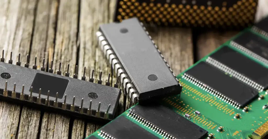
What Are Memory Chips

Memory chips are tiny integrated circuits that store data in electronic devices. They are essential components in computers, smartphones, tablets, and many other digital devices.
Types of Memory Chips
There are two main types of memory chips: volatile and non-volatile. Volatile memory chips, such as RAM (Random Access Memory), lose their data when the power is turned off.
Non-volatile memory chips, such as ROM (Read-Only Memory) and flash memory, retain their data even when the power is off.
- RAM (Random Access Memory): RAM is the computer’s working memory. It stores data that is currently being used by the CPU (Central Processing Unit). RAM is volatile, which means that the data is lost when the computer is turned off.
- ROM (Read-Only Memory): ROM is a type of non-volatile memory that stores data that is permanently programmed into the chip. ROM is typically used to store the computer’s BIOS (Basic Input/Output System), which is the code that starts the computer up and initializes the hardware.
- Flash memory: Flash memory is a type of non-volatile memory that can be erased and reprogrammed. Flash memory is used in a variety of devices, including USB flash drives, solid-state drives (SSDs), and memory cards.
Memory chips come in a variety of sizes and capacities. The size of a memory chip is typically measured in megabytes (MB) or gigabytes (GB). The capacity of a memory chip refers to the amount of data that it can store.
How Are Memory Chips Made?
Delving Deeper into Memory Chip Manufacturing:
Here’s a more detailed explanation of each step in the memory chip making process in the following
Step 1. Silicon Ingots: The Foundation
Ultra-pure silicon is the foundation for memory chips. It’s obtained through a process called the Czochralski process.
Imagine a giant lollipop being pulled from molten sugar. That’s similar to how silicon is grown! Molten silicon is slowly pulled from a crucible, forming a cylindrical single crystal ingot.
These ingots can be surprisingly large, reaching up to 30 cm in diameter!
Step 2. Layered Perfection: Building the Canvas
The silicon ingot is sliced into thin, polished wafers – the canvas for the intricate circuits.
The wafer is placed in a chamber where various deposition techniques are used to create ultra-thin films of materials like:
- Silicon dioxide (SiO2) – acts as an insulator, preventing unwanted electrical flow between circuits.
- Silicon Nitride (Si3N4) – enhances the wafer’s strength and protects underlying layers during processing.
- Polysilicon (Poly-Si) – a conductive layer used for building transistors, the workhorses of memory chips.
- Doping materials (Boron, Phosphorus) – will be used to alter electrical properties later, creating the building blocks of memory cells.
Step 3. Photolithography – The Blueprint Comes to Life
Photolithography is a critical step that transfers the circuit blueprint onto the wafer. Here’s how it works:
- A light-sensitive photoresist is spun onto the wafer, coating it uniformly.
- A mask, containing the intricate circuit patterns, is placed on top of the wafer. This mask acts like a giant stencil.
- Ultraviolet light is shone through the mask. The exposed photoresist hardens, becoming resistant to etching.
- The unexposed photoresist remains unchanged.
Step 4. Etching – Sculpting the Landscape
Powerful chemicals or plasma are used to etch away the unwanted material, following the blueprint defined by the photoresist.
Imagine carving away unwanted material to reveal the underlying design. That’s essentially what etching does.
- The hardened photoresist acts as a barrier, protecting the desired circuit patterns.
- This process sculpts the various layers, forming the foundation for transistors, capacitors, and interconnects that will allow communication between different parts of the chip.
Step 5. Doping and Implantation: Adding the Magic Touch
Doping and implantation are like adding spices to a dish – they alter the electrical properties of silicon to create functional circuits.
Doping: Precisely introducing impurities (dopants) into specific areas of the silicon alters its electrical conductivity.
- Boron creates “p-type” regions with positive charge carriers (holes).
- Phosphorus creates “n-type” regions with negative charge carriers (electrons).
- The combination of p and n type regions forms the basis of transistors, the building blocks of memory cells.
- Ion Implantation: Doping can also be achieved by precisely accelerating ions (charged atoms) and implanting them into the silicon at specific depths. This offers more precise control over doping.
Step 6. Repeat and Refine: Building Floor by Floor
The deposition, photolithography, etching, and doping steps are repeated multiple times, building up the complex 3D structure of the memory chip layer by layer.
Each layer adds specific functionalities like transistors, capacitors, and metal interconnects that allow communication between different parts of the chip.
Imagine building a intricate skyscraper floor by floor. This step is similar, but on a microscopic scale!
How is RAM Made?
RAM, or Random Access Memory, is your computer’s short-term memory. Here’s a breakdown of how this essential component is manufactured:
Part I: From silicon to finished wafer
- Silicon ingots: The journey begins with ultra-pure silicon, extracted from sand. This silicon is grown into cylindrical rods called ingots.
- Photolithography: The ingots are sliced into wafer-thin disks. These wafers become the foundation for the RAM chips. A complex process called photolithography creates a stencil on the wafer’s surface using light-sensitive material (photoresist).
- Photoresist: This stencil defines the intricate patterns of transistors and capacitors that will make up the memory cells.
- Etch: Using the photoresist stencil as a guide, the unwanted silicon is etched away, leaving behind the designed circuit patterns.
Part II: Layering the wafer and completing the circuit
- Aluminum layering: A thin layer of aluminum is deposited on the wafer. This aluminum will become the conductive pathways for electrical signals within the memory chip.
- Passivation layering: A protective layer is applied to insulate the delicate circuitry and prevent contamination.
Part III: Die preparation and testing
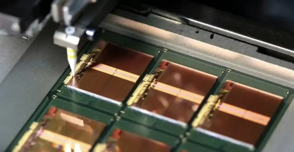
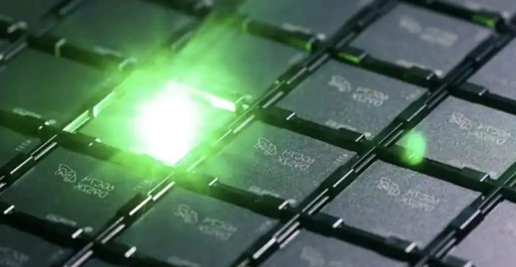
- Encapsulation: The wafer is diced into individual memory chips, each called a die. These dies are then encased in a protective package.
- Electroplating: Electrical connections are formed on the die’s surface using a process called electroplating.
- Trim and form: The individual dice are trimmed to their final size and shape.
- Burn-in testing: The dice undergo rigorous testing to ensure they function properly at high temperatures, revealing any potential defects.
Part IV: Module assembly
- PCB assembly and construction: A Printed Circuit Board (PCB) is prepared, containing the necessary components to connect with the memory chips.
- Screen print: A stencil is used to apply solder paste onto designated locations on the PCB.
- Soldering and attachment: The memory chips (dice) are precisely placed on the PCB, and the solder paste is melted to create a permanent connection.
- Post-assembly quality testing: The completed RAM modules undergo final electrical testing to verify functionality and speed.
- Shipment: Only after passing all inspections, the RAM modules are carefully packaged and shipped for use in computers around the world.
Conclusion
So, the next time you power on your smartphone or computer, take a moment to appreciate the invisible symphony of engineering that allows you to store and access your data with incredible speed and efficiency.
Are you curious to learn more about specific types of memory or how they’re used in different devices? Leave a comment below and let us know what interests you!