Embark on a journey through the realm of electronic component package types, where innovation meets functionality. Understanding these components is crucial for engineers, hobbyists, and anyone interested in electronics.
This comprehensive guide will delve deep into various package types, shedding light on their significance and applications.
Why are Electronic Component Packages Important?
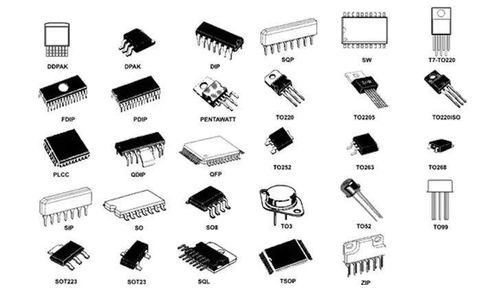
Electronic component packages are vital components in the world of electronics for several reasons:
- Protection: One of the primary functions of electronic component packages is to protect delicate electronic components from environmental factors such as moisture, dust, and mechanical stress. By enclosing components within a package, they are shielded from potential damage, ensuring their longevity and reliability.
- Facilitating Assembly: Electronic component packages play a crucial role in the assembly process of electronic circuits. They provide a standardized form factor and interface, making it easier for manufacturers to integrate components into circuit boards through automated assembly processes.
- Heat Dissipation: Many electronic components generate heat during operation, which can degrade performance or even cause failure if not properly managed. Certain package types are designed with features such as heat sinks or thermal vias to dissipate heat efficiently, maintaining optimal operating temperatures and prolonging component lifespan.
- Electrical Connectivity: Packages serve as interfaces between electronic components and circuit boards, facilitating electrical connections through soldering or other bonding techniques. They ensure reliable electrical contact while minimizing signal interference or loss, crucial for maintaining circuit integrity and performance.
- Miniaturization: As electronic devices become increasingly compact and portable, the demand for smaller and more lightweight components continues to grow. Miniaturized package types, such as chip-scale packages (CSPs) and ball grid arrays (BGAs), enable designers to achieve higher component density and functionality within limited space constraints.
- Standardization and Interoperability: Standardized package formats and footprints enable interoperability between components from different manufacturers, simplifying design processes and promoting compatibility across various electronic systems. This standardization streamlines supply chains and reduces costs associated with component sourcing and inventory management.
Electronic component packages serve as the backbone of modern electronics, providing essential functionalities such as protection, connectivity, and thermal management.
Their significance extends beyond mere enclosures, contributing to the reliability, performance, and innovation of electronic devices across diverse industries and applications.
What Protection Does Electronic Packaging Design Offer?
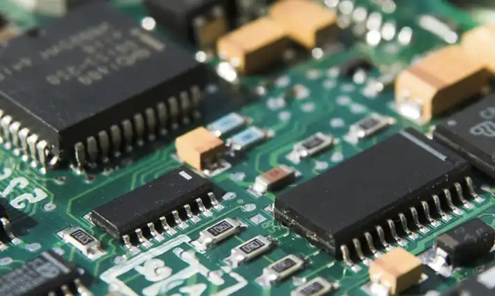
Electronic packaging design offers several layers of protection to ensure the integrity and reliability of electronic components:
- Environmental Protection: Electronic packaging shields components from environmental factors such as moisture, dust, and debris. Sealed packages prevent contaminants from entering sensitive electronic circuits, safeguarding them from corrosion and physical damage.
- ESD Protection: Electrostatic discharge (ESD) can pose a significant threat to electronic components, leading to immediate or latent failures. Packaging designs incorporate ESD protection measures such as conductive or dissipative materials and grounding mechanisms to safely dissipate static charges and prevent damage during handling, assembly, or operation.
- Mechanical Protection: Electronic packaging provides mechanical support and shock absorption to withstand mechanical stresses encountered during shipping, handling, or operation. Robust package designs minimize the risk of physical damage from impacts, vibrations, or flexing, ensuring component reliability in harsh environments.
- Thermal Management: Heat dissipation is critical for maintaining optimal operating temperatures and preventing thermal-induced failures in electronic components. Packaging designs incorporate thermal management features such as heat sinks, thermal pads, or encapsulation materials with high thermal conductivity to efficiently dissipate heat and prevent overheating.
- Tamper Protection: In applications where security is paramount, electronic packaging may include tamper-evident or tamper-resistant features to deter unauthorized access or tampering. These features include sealants, coatings, or physical barriers that indicate if a package has been compromised, ensuring the integrity and confidentiality of enclosed components or data.
By integrating these protection mechanisms into electronic packaging designs, electronic component manufacturers can enhance electronic components’ reliability, durability, and security, ensuring their performance and longevity in diverse operating environments.
Electronic Component Package Types
When it comes to electronic component package types, there’s a wide array of options available, each serving specific purposes and offering unique benefits.
Let’s delve deeper into each type, exploring their characteristics and applications, and helping you understand which one might be the best fit for your needs:
Most Common Electronic Component Packages
Here is the table showing you the most electronic component package types below:
| IC Package Type | Description | Advantages | Disadvantages | Common Applications |
|---|---|---|---|---|
| Dual In-Line Package (DIP) | Featuring two rows of pins, DIP stands as one of the earliest and most widespread package types | Easy to insert into socket connectors on PCB | Bulky and limited pin count; less suited for modern designs | Found in legacy applications and simple circuits |
| Surface Mount Device (SMD) | With solderable pads on the bottom surface, SMD offers a space-saving solution | Compact and lightweight, suitable for automated assembly | Not well-suited for high-power applications | Widely used in general electronics and consumer devices |
| Ball Grid Array (BGA) | BGA boasts solder balls on the bottom surface, ensuring high-performance | High pin count and excellent thermal dissipation | Rework and repair are challenging; manufacturing can be difficult | Primarily used in microprocessors, GPUs, and high-speed applications |
| Quad Flat No-Lead (QFN) | QFN features metal pads on the bottom with no exposed leads, offering good thermal performance | Compact and low profile with superior thermal characteristics | Inspecting solder joints is difficult; not suitable for high power | Commonly employed in power management ICs and RF applications |
| Dual Flat No-Lead (DFN) | DFN, a smaller variant of QFN, comes with fewer pins | Compact, space-saving, and lightweight design | Limited pin count and challenging rework | Often found in mobile devices and small electronics |
| Chip Scale Package (CSP) | CSP, extremely compact and almost the same size as the IC, achieves maximum miniaturization | Space-efficient design with maximum miniaturization | Manufacturing is challenging and may require specialized PCBs | Ideal for smartphones, wearables, and space-constrained applications |
Here are the many different methods for packaging electronic components in the following:
Dual In-line Package (DIP):
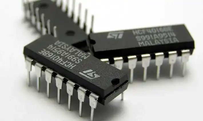
DIP packages are a classic choice, easily recognizable by their two parallel rows of leads. They’re perfect for through-hole mounting, which means they’re suitable for circuits where components are inserted into pre-drilled holes on the circuit board.
DIP packages are commonly used for integrated circuits (ICs) and discrete components like resistors and capacitors. Their straightforward design and ease of handling make them a popular choice for hobbyists and prototyping projects.
Surface-Mount Device (SMD):
SMD packages are all about efficiency and space-saving. With no protruding leads, they’re designed to be mounted directly onto the surface of the circuit board. This makes them ideal for high-density circuit designs where space is at a premium.
SMD components are widely used in modern electronics, from smartphones and tablets to automotive electronics and industrial control systems. Their small size and compatibility with automated assembly processes make them indispensable in today’s electronic manufacturing industry.
Ball Grid Array Package (BGA):
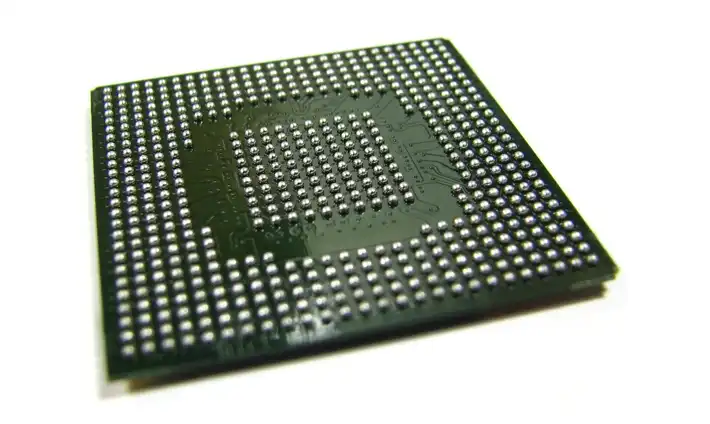
BGA packages take connectivity to the next level with their array of solder balls arranged in a grid pattern beneath the component. This design not only maximizes the number of connections but also enhances thermal and electrical performance.
BGAs are commonly found in advanced microprocessors, graphics processors, and other high-performance integrated circuits where reliability and compactness are paramount. While they may pose challenges during rework and inspection due to their concealed connections, their benefits outweigh the drawbacks in many applications.
Quad Flat Package (QFP):

QFP packages strike a balance between component density and ease of assembly. With flat leads extending from all four sides, they offer ample pin counts while still being relatively straightforward to solder onto the circuit board.
QFPs find widespread use in microcontrollers, memory devices, and other integrated circuits where moderate pin counts are required. Their versatility and compatibility with both automated and manual assembly processes make them a versatile choice for various applications.
Small Outline Integrated Circuit (SOIC):
SOIC packages are compact and efficient, featuring gull-wing leads extending from two opposite sides of the component. They’re a popular choice for a wide range of integrated circuits and discrete components, offering space-saving benefits without sacrificing performance. SOICs are commonly used in consumer electronics, telecommunications equipment, and automotive systems, where reliability and compactness are essential considerations.
Chip-Scale Package (CSP):
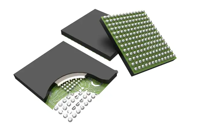
CSP packages take miniaturization to the extreme, with package sizes comparable to the integrated circuit chip itself. These tiny packages offer exceptional space efficiency and thermal performance, making them ideal for portable electronic devices like smartphones, wearables, and IoT devices.
While CSPs may require specialized assembly techniques and handling precautions due to their small size, their benefits in terms of size reduction and performance enhancement are undeniable.
Thin Small Outline Package (SOP/SOIC/SO):
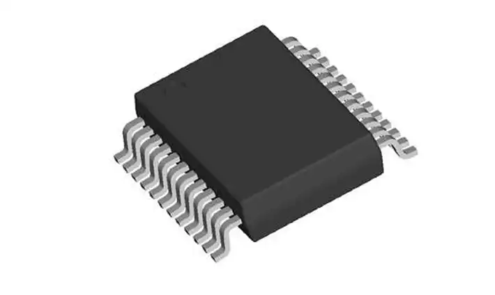
TSOP packages are characterized by their thin, flat leads along two sides of the component, allowing for high component density and reduced profile. They’re commonly used for memory devices like flash memory and dynamic random-access memory (DRAM) in applications where space is limited. TSOPs are found in a wide range of consumer electronics, from digital cameras and MP3 players to set-top boxes and gaming consoles, where compactness and reliability are key considerations.
Tamper-Evident Carton:
Tamper-evident cartons are packaging solutions designed to provide visual indications of tampering or unauthorized access. While not directly housing electronic components, they play a crucial role in protecting the integrity of packaged products, including electronic devices and components. Tamper-evident cartons typically feature seals, tapes, or other closure mechanisms that break or become visibly damaged upon tampering, alerting end-users to potential security breaches.
Quad Flat Non-leaded Package (QFN/LCC)
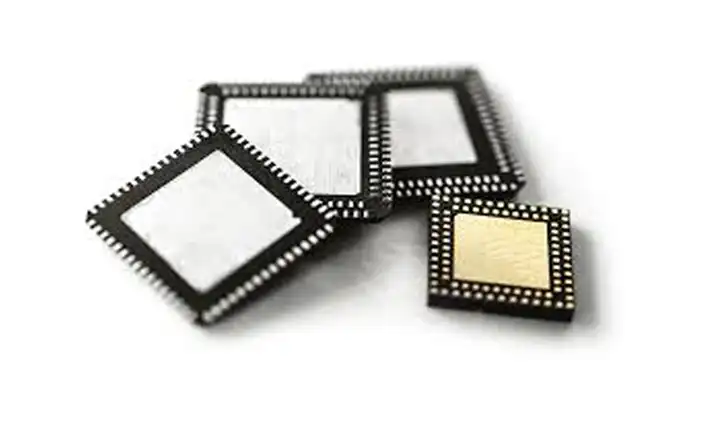
The Quad Flat Non-leaded Package (QFN/LCC) is a surface-mount package that offers a compact and robust solution for integrated circuits (ICs) and other semiconductor devices. Unlike traditional leaded packages, QFN/LCC packages feature exposed pads on the bottom surface instead of leads, allowing for direct soldering to the circuit board. This design eliminates the need for leads, reducing the overall footprint of the package and enhancing thermal performance.
QFN/LCC packages are commonly used in applications where space constraints are critical, such as mobile devices, automotive electronics, and IoT devices. Their low profile and excellent thermal dissipation properties make them an ideal choice for high-density and high-power applications, where reliability and efficiency are paramount considerations.
QFN/LCC packages offer several advantages over traditional leaded packages, including improved electrical performance, enhanced thermal management, and simplified assembly processes. The absence of leads minimizes parasitic inductance and capacitance, resulting in better signal integrity and higher-frequency operation.
IC Package Types
The most common IC package types include
- Dual In-Line Package (DIP)
- Small Outline Package (SOP)
- Thin Small Outline Package (TSOP)
- Quad Flat Package (QFP)
- Quad Flat Package-Extended (QFP-EP)
- Quad Flat No-leads (QFN)
- Ball Grid Array (BGA)
- Micro Ball Grid Array (µBGA)
- Ceramic Ball Grid Array (CBGA)
- Plastic Ball Grid Array (PBGA)
- Fine-Pitch Ball Grid Array (FBGA)
- Chip Scale Package (CSP)
- Dual Flat No-leads (DFN)
- Plastic Leaded Chip Carrier (PLCC)
- Small Outline Transistor (SOT)
- Small Outline Diode (SOD)
- Small Outline J-Lead (SOJ)
- Dual In-line Memory Module (DIMM)
- Single In-line Memory Module (SIMM)
- Quad Flat Package No-lead (QFN-ML)
- Ultra-Thin Quad Flat No-lead (UQFN)
- SOT-23
- SOT-223
- SOT-323
- SOT-363
- SOT-523
Here is an electronic component package types pdf you can view in the following:
How to Choose the Right Electronic Component Package?
Choosing the right electronic component package is crucial for the success of your project, as it impacts factors such as performance, reliability, and ease of assembly. Here are some key considerations to help you make an informed decision:
Application Requirements: Consider the specific requirements of your application, such as operating environment, power requirements, and size constraints. Certain package types may offer better thermal performance or space efficiency, depending on your application’s needs.
Mounting Method: Determine whether you’ll be using through-hole or surface-mount assembly techniques. Through-hole packages like DIP may be more suitable for prototyping or hobbyist projects, while surface-mount packages like SMD offer space-saving benefits and compatibility with automated assembly processes.
Pin Count: Evaluate the number of pins or leads required for your component. Packages with higher pin counts, such as BGAs, offer greater connectivity but may be more challenging to work with during assembly or repair.
Thermal Considerations: Take into account the thermal requirements of your application, especially if your component will be subjected to high temperatures or require efficient heat dissipation. Package types like BGA or QFN with superior thermal characteristics may be preferable for high-power applications.
Manufacturability: Consider the ease of manufacturing and assembly when selecting a package type. Some package types, such as CSP or QFN, may require specialized assembly techniques or equipment, which could impact production costs and lead times.
Rework and Repair: Assess the ease of rework and repair for the chosen package type. Packages like DIP or SOIC may be easier to rework manually, while packages like BGA or CSP may require specialized equipment and expertise for rework or repair.
Compatibility: Ensure compatibility with other components and circuitry in your design. Verify that the chosen package type is compatible with the rest of your components and can be seamlessly integrated into your circuit layout.
FAQs
How do I choose the right package type for my project?
Selecting the appropriate package type depends on various factors, including space constraints, thermal requirements, and assembly processes.
What are the advantages of surface-mount packages over through-hole packages?
Surface-mount packages offer advantages such as smaller footprint, higher component density, and automated assembly, making them preferred choices for modern electronics.
Are there any drawbacks to ball grid arrays (BGAs)?
While BGAs offer numerous benefits, challenges such as rework difficulty and inspection complexity should be considered, especially in prototyping and low-volume production.
Can chip-scale packages (CSPs) replace traditional packages entirely?
While CSPs offer significant advantages in miniaturization, their adoption depends on factors such as cost, reliability, and compatibility with existing manufacturing processes.
How do I interpret package markings?
Package markings typically include information about the component type, manufacturer, date code, and specifications. Consulting datasheets or manufacturer documentation can aid in deciphering these codes accurately.
Conclusion
In conclusion, mastering the intricacies of electronic component package types is essential for anyone venturing into the world of electronics. By understanding the diverse array of package types, their applications, and future trends, enthusiasts can navigate this dynamic landscape with confidence and innovation.