P Channel Mosfet
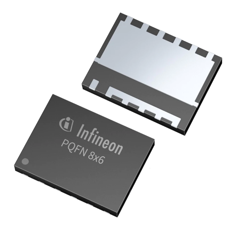
P Channel MOSFET are semiconductor devices that control the flow of current between the source and drain terminals using an electric field applied to a third terminal (gate). They are widely used in electronic circuits due to their efficiency, high switching speed, and ability to handle large currents.
P-channel MOSFETs are complementary to N-channel MOSFETs, offering distinct advantages in specific applications.
P Channel Mosfet Application
P Channel MOSFETs have carved out a distinct niche in electronic circuit design due to their unique characteristics. Their ability to function as high-side switches, where the load is connected directly to the positive power supply, has made them indispensable in various applications.

P-channel MOSFETs are pivotal in BMS circuits. They serve as crucial elements for over-discharge protection, preventing battery damage from excessive current draw. Additionally, they can be configured to provide reverse polarity protection, safeguarding the system from incorrect battery installation.

Precise control over power distribution is essential in many electronic devices. P-channel MOSFETs excel in load switching applications, enabling the selective activation and deactivation of peripherals or subsystems. Their fast switching speeds contribute to efficient power management and system optimization.

In power conversion circuits such as DC-DC converters, P-channel MOSFETs play a vital role. They can be employed in both synchronous and asynchronous configurations to regulate output voltage and current. Their low on-resistance contributes to improved efficiency and reduced power dissipation.

While primarily associated with N-channel MOSFETs, P-channel devices also have a role in motor drive systems. They can be used in conjunction with N-channel MOSFETs to create H-bridge configurations, facilitating bidirectional motor control.

PMICs often incorporate P-channel MOSFETs for various functions including load switching, power sequencing, and overcurrent protection. Their integration into a single chip simplifies circuit design and reduces component count.

The automotive industry leverages P-channel MOSFETs extensively. They are found in a wide range of applications, from powertrain systems to body electronics and infotainment systems. Their robustness and reliability make them suitable for the demanding operating conditions encountered in automotive environments.
P Channel MOSFETs

P Channel Mosfet - STD35P6LLF6
The STD35P6LLF6 is a P-channel MOSFET manufactured by STMicroelectronics. It’s designed for applications requiring high current handling and fast switching speeds. Key features include:
- 60V drain-source voltage (Vds): Capable of handling moderate voltage levels.
- 35A drain current (Id): Designed for high current applications.
- Low on-resistance (Rds(on)): Improves efficiency by minimizing power dissipation.
- STripFET™ F6 technology: Offers enhanced performance and reliability.
- DPAK package: Compact and easy to mount.

P Channel Mosfet - IRF7416TRPBF
The IRF7416TRPBF is a 30V, 10A P-channel MOSFET from Infineon Technologies. It’s part of their HEXFET family known for high efficiency and low on-resistance. This device is optimized for high-density applications requiring small size and high performance. Key features of the IRF7416TRPBF:
- 30V drain-source voltage: Capable of handling moderate voltage levels.
- 10A drain current: Designed for medium current applications.
- Extremely low on-resistance: Improves efficiency and reduces power dissipation.
- Small package size: Ideal for high-density circuit boards.
- Fast switching speeds: Suitable for high-frequency applications.

P Channel Mosfet - Si7281DP
The Si7281DP is a 50V, 22A P-channel MOSFET from Vishay. It features a compact SO-8 package and a low on-resistance of 2.5mΩ, making it suitable for high-efficiency power switching applications. The Si7281DP is also RoHS compliant and halogen-free. Key features:
- 50V drain-source voltage
- 22A drain current
- 2.5mΩ on-resistance
- SO-8 package
- RoHS compliant and halogen-free

P Channel Mosfet - BSP3010L
The BSP3010L is a 30V, 10A P-channel MOSFET from Infineon Technologies. It features a low on-resistance of 2.9mΩ and a compact DPAK package, making it suitable for high-efficiency power switching applications in space-constrained environments. The BSP3010L is also AEC-Q101 qualified for automotive applications. Key features:
- 30V drain-source voltage
- 10A drain current
- 2.9mΩ on-resistance
- DPAK package
- AEC-Q101 qualified

P Channel Mosfet - IRL520P
The IRL520P is a 50V, 5.2A P-channel MOSFET from Infineon Technologies. It features a low on-resistance of 3.9mΩ and a compact SO-8 package, making it suitable for cost-effective power switching applications. The IRL520P is also RoHS compliant and halogen-free. Key features:
- 50V drain-source voltage
- 5.2A drain current
- 3.9mΩ on-resistance
- SO-8 package
- RoHS compliant and halogen-free
What is P Channel Mosfet?
A P-Channel MOSFET (Metal-Oxide-Semiconductor Field-Effect Transistor) is a type of MOSFET where the majority carriers are holes. These devices are widely used in electronic circuits for switching and amplifying signals. They are an essential component in various applications, including power management, signal processing, and digital electronics.
Structure of P Channel Mosfet

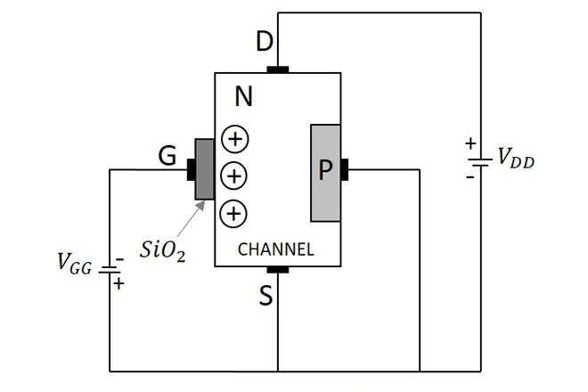
The structure of a P-Channel MOSFET consists of several key elements:
- Substrate: The P-Channel MOSFET has an N-type substrate.
- Source and Drain: The source and drain are heavily doped P+ regions embedded in the N-type substrate.
- Gate: The gate is insulated from the channel by a thin layer of silicon dioxide (SiO2). It is made of polycrystalline silicon or metal.
- Channel: The channel is the region between the source and drain, where current flows when the MOSFET is turned on. In a P-Channel MOSFET, the channel is formed by P-type material.
- Body: The body is the part of the MOSFET that forms the junction with the source and drain. For P-Channel MOSFETs, the body is typically connected to the source.
When a negative voltage is applied to the gate relative to the source, it creates an electric field that attracts holes into the channel region, allowing current to flow from the source to the drain.
P Channel Mosfet Symbol

How to Test P Channel Mosfet?
Testing a P-Channel MOSFET can be done using a multimeter. Here are the steps:
- Identify the Terminals: Determine the source, drain, and gate terminals using the datasheet or markings on the MOSFET.
- Set Multimeter: Set the multimeter to the diode test mode.
- Check Gate to Source: Place the positive probe on the source and the negative probe on the gate. A good MOSFET will show a high resistance or no conduction in this configuration.
- Check Gate to Drain: Move the negative probe to the drain while keeping the positive probe on the source. A good MOSFET will again show high resistance.
- Check Source to Drain: Swap the probes (negative on source, positive on drain) and you should see no conduction.
- Check Forward Conduction: Finally, check the forward conduction by placing the positive probe on the source and the negative on the drain while applying a negative voltage to the gate (you can do this by connecting the gate to the negative probe). The multimeter should show low resistance, indicating the MOSFET is conducting.
How Does P Channel Mosfet Work?

The operation of a P-Channel MOSFET involves the following principles:
Off State: When no voltage or a positive voltage is applied to the gate relative to the source, the P-Channel MOSFET is in the off state. The absence of holes in the channel region means no current flows between the source and the drain.
On State: When a negative voltage is applied to the gate relative to the source, it creates an electric field that attracts holes into the channel region. This forms a conductive path between the source and the drain, allowing current to flow. The amount of current flow is controlled by the gate-source voltage (V_GS).