The world around us is becoming increasingly reliant on technology, and at the heart of this dependence lies the unsung hero: the integrated circuit (IC). But what exactly is an IC, and how does it come to be? This blog post dives into the fascinating world of integrated circuit design, exploring the process behind these miniature marvels.
What is an Integrated Circuit?
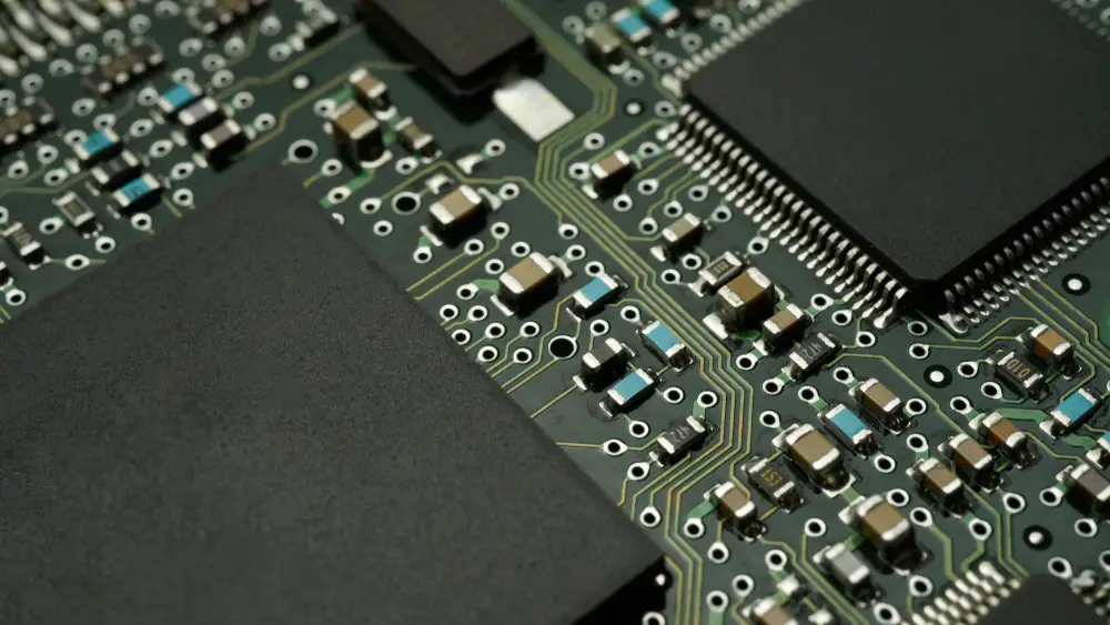
An integrated circuit, also known as a microchip or chip, is a microscopic network of electronic components like transistors, resistors, and capacitors built onto a single piece of semiconductor material, typically silicon. These components are interconnected to perform specific electronic functions. Imagine a city built on a miniature scale, where houses represent transistors, roads represent wires, and power plants represent power sources. An IC miniaturizes these elements into an incredibly small space, allowing for complex functionality in a compact package.
Why is Integrated Circuit Design Important?
Integrated circuit design is fundamental to modern electronics. It forms the foundation for everything from smartphones and laptops to medical devices and automobiles. The ability to pack immense processing power into tiny chips has revolutionized how we live, work, and communicate. Advancements in IC design continue to drive miniaturization, leading to more powerful and efficient devices.
What is Integrated Circuit Design
Integrated circuit design (IC design) is a specialized field within electronics engineering. Electronics engineers design circuits, which are networks of electronic components that work together to achieve a particular goal.
Simple examples include circuits that add or multiply numbers. More complex examples include microprocessors, the brains of modern computers, that can follow instructions and perform many complex tasks.
IC design takes this concept to a whole new level of miniaturization. Instead of building circuits using separate electronic components, IC design crams these tiny building blocks, like transistors and resistors, onto a single piece of silicon, creating microscopic versions of those circuits. This allows for incredibly complex functionality to be packed into a very small space.
Integrated Circuit Engineering

Integrated Circuit (IC) engineering, also known as integrated circuit design or chip design, is a fascinating field within electronics engineering. It focuses on the creation of those tiny marvels of technology we call integrated circuits, or ICs, often referred to simply as chips.
Radio Frequency Integrated Circuit Engineering
Radio Frequency Integrated Circuit (RFIC) engineering is a specialized field within IC engineering that focuses on designing integrated circuits specifically for operating at radio frequencies (RF). These frequencies typically range from tens of kilohertz (kHz) to tens of gigahertz (GHz).
Here’s how RFIC engineering differs from regular IC engineering:
- Focus on High Frequencies: Unlike standard ICs that deal with lower frequencies, RFICs handle high-frequency signals used in radio communication, Bluetooth, Wi-Fi, and many other wireless technologies.
- Specialized Components: RFICs utilize special components like inductors, capacitors, and transistors designed to function effectively at high frequencies. These components often require careful layout considerations to minimize parasitic effects that can degrade signal quality.
- Electromagnetic Considerations: RF signals are susceptible to electromagnetic interference (EMI) and require careful design to minimize signal distortion and crosstalk. RFIC engineers need a strong understanding of electromagnetic theory and how it affects circuit behavior at high frequencies.
- Mixed-Signal Design: RFICs often combine both analog and digital circuits on a single chip. Analog circuits handle the actual RF signals, while digital circuits perform tasks like signal processing, modulation, and demodulation.
RFIC Design Challenges:
Designing RFICs presents unique challenges compared to standard ICs:
- Noise: At high frequencies, noise becomes a significant concern that can degrade signal quality. RFIC engineers need to implement techniques like noise filtering and shielding to minimize noise impact.
- Power Consumption: RF circuits can be power-hungry, especially at high frequencies. Optimizing power consumption is crucial for battery-powered devices.
- Integration: Integrating various analog, digital, and RF components on a single chip requires careful layout and design techniques to ensure proper signal integrity and minimize interference.
Applications of RFICs:
RFICs are essential components in a wide range of wireless technologies:
- Mobile Phones: RFICs handle signal transmission and reception in cellular communication.
- Wireless Networking: Wi-Fi routers and access points utilize RFICs for data transmission.
- Bluetooth Devices: RFICs enable wireless communication between Bluetooth devices.
- Satellite Communication: RFICs are crucial components in satellite communication systems.
- Radar and Navigation Systems: RFICs are used in radars and GPS receivers.
The Future of RFIC Engineering:
The demand for high-speed wireless technologies continues to grow, driving innovation in RFIC engineering. Emerging trends include:
- Millimeter-wave (mmWave) ICs: These RFICs operate at even higher frequencies, enabling faster data rates and supporting applications like 5G and future wireless technologies.
- Low-Power RFIC Design: As battery life becomes increasingly important, RFIC engineers are constantly striving to reduce power consumption in RF circuits.
- Integration with other Technologies: RFICs are being integrated with other technologies like sensors and microprocessors to create more complex and versatile wireless devices.
A Peek Inside the Integrate Circuit Design Process
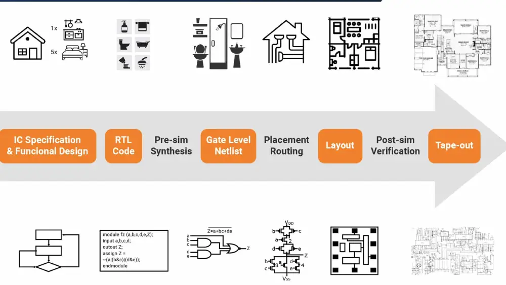
Designing an IC is a complex and meticulous process that can be broadly divided into three stages: functional design, circuit design, and physical design.
- Functional Design: This initial stage defines the desired functionality of the IC. Engineers meticulously describe the operations the circuit needs to perform, similar to an architect creating a blueprint for a building.
- Circuit Design: Here, the blueprint translates into electrical specifications. Engineers select and arrange transistors, resistors, and capacitors to achieve the defined functionality. Computer-aided design (CAD) tools are crucial in this stage for simulating circuit behavior and ensuring proper operation.
- Physical Design: The magic of miniaturization happens here. Engineers convert the electrical schematic into a physical layout on the silicon chip. This layout defines the placement and interconnection of all components, ensuring they fit within the designated space while maintaining functionality.
The IC Design Toolbox
IC designers employ a variety of sophisticated tools and methodologies to create these intricate circuits. Here are some key elements:
- Hardware Description Languages (HDLs): These specialized languages, like Verilog and VHDL, allow engineers to describe the desired functionality of the circuit in a textual format. These descriptions can then be translated into circuit schematics.
- Computer-Aided Design (CAD) Tools: EDA (Electronic Design Automation) software plays a vital role. These tools help with circuit simulation, layout design, and verification throughout the design process.
- Design for Manufacturability (DFM): ICs are manufactured using a complex photolithography process. Designing circuits that can be efficiently manufactured is crucial, and DFM techniques ensure the manufacturability of the design.
How to Design an Integrate Circuit
Integrated circuit (IC) design is a fascinating journey that transforms ideas into the tiny powerhouses that drive modern technology. This process can be visualized as a series of steps, gradually refining a high-level concept into a detailed blueprint for a silicon chip.
1. Architectural Design: Defining the “What”
The first step lays the foundation. Here, engineers define the chip’s desired functionality. What does it need to do? How fast and efficient should it be? This initial brainstorming considers the bigger picture, focusing on the “what” rather than the “how.”
2. Logic/Circuit Design: Assembling the Building Blocks
Think of this stage as constructing a miniature city. Pre-designed components like memory units and processors are assembled to achieve the required functionality. Software automates the process, translating high-level descriptions into the underlying circuitry. Simulations ensure everything works as planned, with different simulators used for digital or analog parts.
3. Physical Design: Bringing the Blueprint to Life
Now, the blueprint gets a physical form. This stage involves creating the actual layout of the circuit elements on the silicon wafer. Imagine meticulously placing and connecting tiny building blocks to fit within a designated space. Custom design techniques come into play if pre-existing components need modifications.
4. Physical Verification: Ensuring It Works in the Real World
The manufacturing process itself can add slight imperfections. Here, engineers account for these realities by modeling factors like added resistance and signal interference. Additionally, strict design rules are checked to ensure the layout is manufacturable.
5. Signoff: The Final Seal of Approval
This is the final checkpoint before the design heads to production. Every critical parameter is meticulously verified for performance and manufacturability. Think of it as a final quality control inspection before giving the green light.
Beyond the Basics: Addressing Advanced Challenges
As technology advances, additional considerations arise. Miniaturization introduces physical effects like significant wire resistance, impacting circuit behavior. To address this, these “late effects” are modeled early on, ensuring the design accounts for them.
Shifting Left: Thinking Ahead for Success
Modern design approaches emphasize a “Shift-Left” philosophy. This means considering aspects like testing and power consumption throughout the process, not just at the end. This proactive approach requires sophisticated tools and design flows to support it.
The IC design flow is a complex and fascinating dance between creativity, meticulous planning, and cutting-edge technology. By understanding these steps, we gain a deeper appreciation for the tiny chips that power our world.
Very Large Scale Integrated Circuit Design
Very-Large-Scale Integration (VLSI) circuit design is a specific branch within the overall world of IC design that deals with creating incredibly complex integrated circuits. Here’s a breakdown of what VLSI entails:
Scale Matters: The defining characteristic of VLSI is the sheer number of transistors crammed onto a single chip. We’re talking millions, or even billions, compared to the thousands or less in simpler ICs. This miniaturization allows for chips with immense processing power and functionality.
Design Challenges: Packing so many elements onto a tiny space presents unique challenges. VLSI designers need to consider factors like:
- Heat Dissipation: More transistors generate more heat, which can damage the chip. Techniques like heat sinks and power-efficient design are crucial.
- Signal Integrity: Miniaturization can introduce signal interference. Careful layout and design strategies are needed to ensure clear and reliable signal transmission.
Design Tools and Techniques: VLSI design relies heavily on sophisticated computer-aided design (CAD) tools to handle the complexity and ensure layout efficiency. Specialized software helps with tasks like simulation, placement, and routing of millions of components.
Applications: VLSI circuits are the heart of modern technology. They power everything from smartphones and laptops to complex medical devices and high-performance computing systems. The ability to integrate vast amounts of processing power into a compact chip is a key driver of technological advancements.
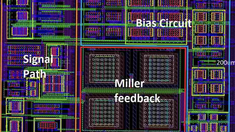
Layout Design of Integrated Circuits Example
Imagine a simple inverter circuit, one of the fundamental building blocks in digital logic. Here’s a breakdown of how its layout design might look:
1. Schematic Representation:
First, we have the schematic diagram, which resembles a blueprint using symbols to represent transistors, resistors, and their connections. This schematic defines the functionality of the circuit.
2. Transistor Layout:
Each transistor in the schematic translates to a specific geometric layout on the silicon chip. These layouts involve carefully designed shapes for different regions of the transistor (source, drain, gate, etc.) that control the flow of current.
3. Interconnections:
The wires connecting the components in the schematic also need to be translated into a physical layout. These wires are represented by thin lines of metal deposited on the chip surface. Careful planning is required to ensure proper spacing and signal integrity.
4. Additional Considerations:
- Power and Ground: Separate layers are dedicated for supplying power and providing a ground reference for the circuit. These layers are typically made of metal.
- Pads: Connection points for external signals are represented by pads located at the periphery of the chip. These pads allow the chip to interface with other components.
- Design Rules: Strict design rules govern the minimum width and spacing of metal lines, the size of transistors, and other layout features. These rules ensure manufacturability and proper circuit operation.
Visualization Tools:
While the actual layout can be quite intricate, Electronic Design Automation (EDA) tools help visualize and manage the design process. These tools allow engineers to:
- Place and route circuit elements on the chip surface.
- Perform simulations to verify circuit functionality with the physical layout.
- Ensure adherence to design rules for manufacturability.
Importance of Layout Design:
The layout design significantly impacts the performance and efficiency of the final chip. Key factors include:
- Propagation Delay: The time it takes for a signal to travel through the circuit, which is influenced by the length and width of metal lines.
- Area Utilization: Efficient use of chip space is crucial, as smaller chips are generally cheaper to manufacture.
- Crosstalk: Unwanted signal coupling between nearby wires, which can be minimized through proper layout techniques.
Analog Integrated Circuit Design
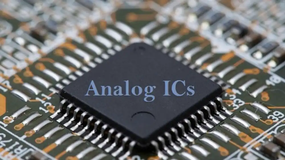
Here is the analysis and design of analog integrated circuits. Analog integrated circuit (IC) design is a specialized field within IC design that focuses on creating circuits that deal with continuous signals, as opposed to the digital world of 0s and 1s.
Here’s a closer look at what makes analog IC design unique:
Continuous World: Analog circuits handle signals that can vary continuously over a range. This is in contrast to digital circuits, which work with discrete voltage levels representing 0 or 1. Examples of analog signals include audio signals (sound) or sensor readings (temperature, light).
Building Blocks: The fundamental components of analog ICs are different from their digital counterparts. Transistors are still key players, but analog designs utilize them in ways that exploit their ability to amplify and manipulate continuous signals. Other important components include resistors, capacitors, and inductors, which play crucial roles in filtering, amplifying, and shaping analog signals.
Design Challenges: Analog design presents its own set of challenges:
- Noise Control: Analog signals are more susceptible to noise and interference compared to digital signals. Careful design techniques and component selection are necessary to minimize noise and ensure accurate signal processing.
- Linearity: Maintaining a linear relationship between the input and output signals is crucial in many analog circuits. Non-linearities can introduce distortion in the processed signal.
Applications: Analog ICs are essential components in various electronic systems. They are widely used in:
Signal Processing: Amplifiers, filters, and converters that form the backbone of audio and video equipment, communication systems, and sensor interfaces.
Power Management: Regulators, converters, and chargers that control and manage power supplies in devices ranging from portable electronics to power grids.
Analog vs. Digital Design: While the worlds of analog and digital design are distinct, there’s increasing convergence. Mixed-signal ICs combine both analog and digital circuits on a single chip, enabling more complex functionalities in a compact space. For example, modern audio chips might include both analog components for signal processing and digital parts for data conversion and compression.
Conclusion: The Invisible Force Shaping Our World
Integrated circuit design is an engineering marvel that has transformed our world. The tiny chips we take for granted are the result of meticulous planning, powerful tools, and cutting-edge research. As IC design continues to evolve, we can expect even more remarkable advancements that will shape the future of technology.