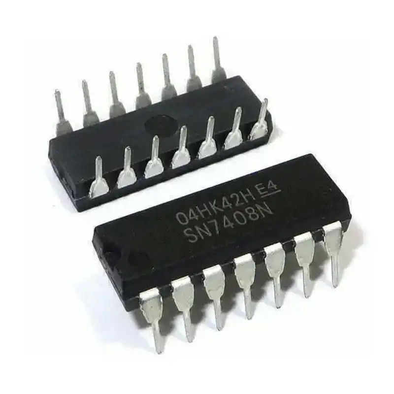
7408 Integrated Circuit
The 7408 integrated circuit is a quad 2-input AND gate, essential for digital logic applications. It operates within a voltage range of 4.75V to 5.25V and is widely used in computing, control systems, and electronic projects for its reliability and performance.
7408 Integrated Circuit
The 7408 integrated circuit is a quad 2-input AND gate, containing four independent AND gates in a single package. It is a part of the 7400 series of TTL (Transistor-Transistor Logic) ICs, known for their robustness and wide usage in digital electronics. The 7408 operates with a power supply voltage ranging from 4.75V to 5.25V, making it suitable for various logic applications.
Order the 7408 IC now to build reliable and efficient digital circuits for your projects!

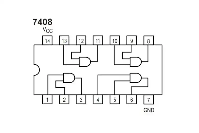
7408 Integrated Circuit Diagram
The 7408 integrated circuit is a quad 2-input AND gate, meaning it contains four independent AND gates in one package. Each gate has two inputs and one output. Here’s a simplified description of its pin configuration and a basic diagram representation:
Pin Configuration:
- Pin 1: Input A1
- Pin 2: Input B1
- Pin 3: Output Y1
- Pin 4: Input A2
- Pin 5: Input B2
- Pin 6: Output Y2
- Pin 7: Ground (GND)
- Pin 8: Output Y3
- Pin 9: Input B3
- Pin 10: Input A3
- Pin 11: Output Y4
- Pin 12: Input B4
- Pin 13: Input A4
- Pin 14: Positive Supply Voltage (Vcc)
Explanation of the Gates:
- Gate 1: Inputs A1 (Pin 1), B1 (Pin 2); Output Y1 (Pin 3)
- Gate 2: Inputs A2 (Pin 4), B2 (Pin 5); Output Y2 (Pin 6)
- Gate 3: Inputs A3 (Pin 10), B3 (Pin 9); Output Y3 (Pin 8)
- Gate 4: Inputs A4 (Pin 13), B4 (Pin 12); Output Y4 (Pin 11)
Each gate performs a logical AND operation, where the output is high (1) only when both inputs are high (1). This IC is commonly used in digital logic circuits where multiple AND operations are required.
Get the 7408 IC now to implement efficient AND gate logic in your digital projects!