3D Integrated Circuits: Revolutionizing Performance and Miniaturization
Ready to unlock the potential of 3D ICs? Explore the latest advancements and discover how this revolutionary technology can transform your next project. Download our white paper on 3D IC design principles today!
Three Dimensional Integrated Circuit Design
Three-Dimensional Integrated Circuits (3D ICs) are a revolutionary approach to chip design that stacks multiple layers of silicon wafers on top of each other, vertically integrating them into a single functional unit.
3D Integrated Circuit FAQs
What are 3D Integrated Circuits
A 3D Integrated Circuit (3D IC) is a cutting-edge chip design that takes traditional two-dimensional (2D) chips to a whole new level.
Imagine a tiny skyscraper for computer chips, where instead of everything being laid out flat, multiple layers of silicon wafers are stacked on top of each other and interconnected vertically.
Benefits of 3D IC Design
- Reduced Size and Weight: By stacking components vertically, 3D ICs can achieve significantly smaller footprints compared to 2D designs. This is crucial for miniaturization in electronics, leading to more compact and portable devices.
- Increased Performance: Shorter distances between components in a 3D stack translate to faster signal transmission and reduced latency. This can significantly improve processing speed and overall system performance.
- Enhanced Functionality: 3D integration allows for the combination of different types of technologies on separate layers. Imagine stacking logic circuits with high-density memory or integrating specialized processors for specific tasks. This enables the creation of highly functional and versatile chips.
- Improved Power Efficiency: Shorter connections lead to lower power consumption due to reduced signal resistance. Additionally, 3D stacking allows for better thermal management, further contributing to power efficiency.
how does 3D Integrated Circuit work
A 3D Integrated Circuit (3D IC) functions by stacking multiple layers of silicon wafers vertically and then interconnecting them to create a single, powerful unit.
Here’s a deeper look at how it works:
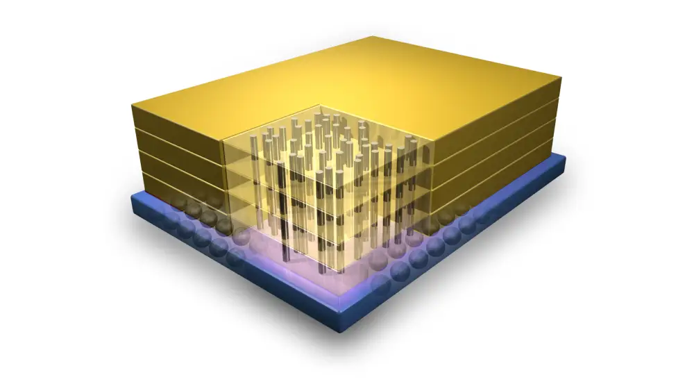
The Building Blocks:
- Wafers: These are thin slices of silicon, the foundation upon which electronic circuits are built. In 3D ICs, individual wafers can contain logic circuits, memory, or other specialized functions.
- Through-Silicon Vias (TSVs): Imagine microscopic tunnels. TSVs are tiny electrical connections that pierce through the silicon wafers, enabling vertical communication between layers. They’re crucial for data to flow between components stacked on top of each other.
- Bonding Techniques: The stacked wafers need to be securely held together. Techniques like wafer bonding use heat, pressure, or adhesives to create a strong connection between the layers.
The Working Process:
- Individual Wafer Fabrication: Each wafer undergoes a separate manufacturing process to create the desired electronic circuits or components. This involves etching patterns, depositing materials, and forming electrical connections, similar to traditional 2D chip fabrication.
- Wafer Stacking and Bonding: The processed wafers are meticulously aligned and then bonded together using techniques mentioned earlier. Precision is key to ensure proper alignment of electrical components across layers.
- Vertical Interconnection: TSVs are created to establish electrical pathways between components on different layers. This allows signals and data to flow seamlessly across the vertical stack.
- Packaging and Testing: The completed 3D IC is packaged and undergoes rigorous testing to ensure functionality and performance.
Benefits in Action:
- Reduced Distance, Faster Speeds: Compared to traditional 2D chips with longer on-chip connections, the shorter distances between components in a 3D stack translate to faster signal transmission and lower latency. This leads to significant performance improvements.
- Functional Specialization: Different layers can be dedicated to specific functions. Imagine stacking a layer with high-performance processors on top of a layer with high-density memory. This allows for optimized performance and efficient utilization of space.
- Miniaturization: By stacking components vertically, 3D ICs achieve a smaller footprint compared to 2D designs with sprawling layouts. This is crucial for creating compact and portable electronic devices.
Challenges and Considerations:
- Manufacturing Complexity: Building 3D ICs is more intricate than traditional methods. Precise wafer alignment, creating reliable TSVs, and managing heat dissipation within the stacked layers pose significant challenges.
- Design Constraints: Designing 3D ICs requires specialized software tools to handle the complexities of 3D layouts, power delivery, and thermal considerations. This is an evolving field, and design tools are continuously being developed.
- Cost Factors: While offering long-term benefits, the advanced manufacturing processes for 3D ICs can currently be more expensive compared to traditional 2D fabrication.
3D Integrated Circuits represent a significant advancement in chip design. By leveraging these techniques, we can create faster, more powerful, and miniaturized electronics for various applications.